

Starter kit board overview
Chapter 1. Starter kit board overview
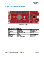
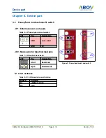
Starter kit board exterior
Figure 1: Starter Kit board
Starter kit board features
Table 1: Main features of starter Kit board
Main features
Specifications
Note
MCU
A34M418YLN
ARM CORTEX-M4F
Operating clock
8 MHz/32.768 KHz
Crystal Main/Sub
ROM
512 KB/32 KB flash ROM
Code / Data
RAM
64 KB
Communication port
USB 2.0
Mini USB Type B 5-pin
Debugging port
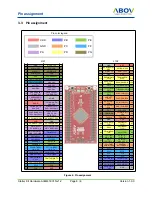
SWD / JTAG
10-pin Connector
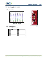
Input buttons
1 reset & 1 event input
TACT Switch
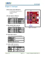
Main features
Specifications
Note
MCU
A34M418YLN
ARM CORTEX-M4F
Operating clock
8 MHz/32.768 KHz
Crystal Main/Sub
ROM
512 KB/32 KB flash ROM
Code / Data
RAM
64 KB
Communication port
USB 2.0
Mini USB Type B 5-pin
Debugging port
SWD / JTAG
10-pin Connector
Input buttons
1 reset & 1 event input
TACT Switch
Starter Kit Hardware A34M418YLN v1.2
Page 4 / 8
Version 1.0.0