78 SBC347A 3U VPX Single Board Computer
Publication No. 500-9300527837-000 Rev. A.0
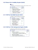
6.62 SSD Erase Control Register (0x6BF)
To trigger a hardware erase, bit 0 must be written with a ‘1’, ‘0’, ‘1’ pattern on
consecutive write cycles to this register. This is to protect against ‘accidental’ erase
functions. The value read from this register represents the state of the output, not
the last value written.
6.63 SSD Cache Flush Control Register (0x6C0)
Bit 0 directly controls the Cache Flush pin of the SSD device.
6.64 VPX Control Register (0x6C1)
The NVMRO Override bit can only be set when the SBC347A is the VPX System
Controller (the VPX_SYSCON pin is set low).
6.65 Scratchpad Register (0x6C6)
This generic read/write register is available to software to validate FPGA access.
It returns 0xFF by default.
Bits
Read/Write Description
Default
7 to 1
Read only SSD7 to SSD1 hardware erase:
SSD7 to SSD1 are not supported.
0 = Hardware erase not available
0000000
b
0
Read/Write SSD0 hardware erase:
0 = Hardware Erase pin active
1 = Hardware Erase pin negated
0
Bits
Read/Write Description
Default
7 to 1
Read only
SSD7 to SSD1 cache flush:
SSD7 to SSD1 are not supported.
0 = Cache flush not available
0000000
b
0
Read/Write SSD0 cache flush:
0 = Cache Flush pin active
1 = Cache Flush pin negated
0
Bits
Read/Write Description
Default
7 to 5
Read only
Reserved
000
b
4
Read/Write VPX Maskable Reset mask:
1 = SBC347A resets when it sees an active low signal on the Maskable Reset backplane pin
0 = SBC347A does
not
reset when it sees an active low signal on the Maskable Reset
backplane pin
0
3
Read/Write VPX Maskable Reset out:
1 = SBC347A drives the Maskable Reset backplane signal low
0 = SBC347A does not drive the Maskable Reset backplane pin (high Z)
0
2
Read/Write NVMRO override:
1 = SBC347A drives the NVMRO backplane signal low
0 = SBC347A does not drive the NVMRO backplane signal (high Z)
0
1 and 0
Read only
Reserved
00
b

