background image

Half-Size CPU Card 

S B C - 6 5 7 B   /   H S B - 6 5 7 I


Chapter4 Drivers Installation


4 - 2


The SBC-657B / HSB-657I comes with a CD-ROM that contains 
most of drivers and utilities of your needs. 

There are several installation ways depending on the driver package 
under different Operating System application.   


Please follow the sequence below to install the drivers: 

Step 1 – Install System Driver 

Step 2 – Install VGA Driver 

Step 3 – Install LAN Driver 

For installation procedures of each driver, you may refer to section 
4.1-4.2. 


Summary of Contents for SBC-657B

Page 1: ...SBC 657B HSB 657I VIA C3 Eden CPU Half Size CPU Card With LCD Ethernet PC 104 CompactFlash USB SBC 657 Rev B HSB 657I Rev A Manual 1 st Ed Nov 2003 ...

Page 2: ...ided in this manual is intended to be accurate and reliable However the original manufacturer assumes no responsibility for its use or for any infringements upon the rights of third parties that may result from its use The material in this document is for product information only and is subject to change without notice While reasonable efforts have been made in the preparation of this document to ...

Page 3: ...properties of their respective owners l Award is a trademark of Award Software International Inc l CompactFlash is a trademark of the Compact Flash Association l Microsoft Windows is a registered trademark of Microsoft Corp l IBM PC AT PS 2 and VGA are trademarks of International Business Machines Corporation ...

Page 4: ...e following materials have been shipped 1 SBC 657B HSB 657I Half Size CPU Card 1 Quick Installation Guide 1 CD ROM for manual in PDF format and drivers 1 Short copper and support 1 Jumper Cap 1 Cable Accessory If any of these items should be missing or damaged please contact your distributor or sales representative immediately ...

Page 5: ...awing 2 7 2 4 List of Jumpers 2 11 2 5 List of Connectors 2 12 2 6 Setting Jumpers 2 13 2 7 COM2 Ring signal select JP1 2 14 2 8 Clear CMOS JP2 2 14 2 9 RS 232 422 485 Setting JP4 2 14 2 10 RS 232 422 485 Setting JP5 2 15 2 11 LCD Shift Clock Select JP6 2 15 2 12 LCD Voltage Setting JP7 2 15 2 13 Power Connector ATX Power PWR1 2 16 2 14 FAN Connector CN1 2 16 2 15 Keyboard and Mouse Connector CN2 ...

Page 6: ...6 COM2 RS 232 422 485 Serial Port Connector CN14 2 24 2 27 VGA Display Connector CN15 2 25 2 28 TTL_LCD Connector CN16 CN17 2 25 2 29 Channel 1 LVDS Connector CN18 2 27 2 30 Channel 2 LVDS Connector CN19 2 27 2 31 Backplane ATX Power Connecotr CN24 2 28 2 32 Internal Mouse Connector CN25 2 28 2 33 Internal Keyboard Connector CN26 2 28 Chapter 3 Award BIOS Setup 3 1 System test and initialization 3...

Page 7: ...ncy Voltage Control 3 13 3 11 Load Fail Safe Defaults 3 14 3 12 Load Optimized Defaults 3 14 3 13 Set Supervisor User Password 3 14 3 14 Save Exit setup 3 15 3 15 Exit Without Saving 3 15 Chapter 4 Driver Installation 4 1 Installation 1 4 3 4 2 Installation 2 4 4 Appendix A Programming the WatchDog Timer Programming A 2 ...

Page 8: ...Half Size CPU Card S B C 6 5 7 B H S B 6 5 7 I Chapter 1 General Information 1 1 General Information Chapter 1 ...

Page 9: ...6 bit Also supporting CRT and LCD to display at the same time offers wider media applications One RJ 45 Ethernet connector comes with a maximum data transfer rate of 100MB per seco nd The 7 3 x 4 8 computer board is connected to the infinite LAN world Four serial ports are designed particularly for industry standard applications and offering various devices connection ability And four USB ports pr...

Page 10: ...pter 1 General Information 1 3 1 2 Features Supports VIA C3 Processor up to 800MHz Integrated AGP 4X 2D 3D graphic accelerator 36 bit TTL LVDS TFT LCD 10 100Mbps Fast Ethernet Supports Type II CompacFlash Memory PC 104 expansion interface ISA interface ...

Page 11: ...ype II CompactFlash Slot l Watchdog timer Generate a system reset l Ethernet RTL 8139D 10 100Base T RJ 45 Ethernet connector x 1 l Expansion Interface ISA interface PC 104 socket l Battery Lithium battery l Power supply voltage 5V 12V 5VSB ATX l Operating temperature 32 to 140 F 0 to 60 C l Board size 7 3 L x 4 8 W 185 mm x 122 mm l Gross Weight 0 66lb 0 3kg Display l Chipset VIA VT8606 l Memory s...

Page 12: ... CRT l LCD Interface 18 36 bit TTL LVDS TFT DSTN LCD l Supports CRT and LCD simultaneous display I O l MIO EIDE UDMA100 x 1 FDD x 1 RS 232 422 485 x 1 RS 232 x 3 LPT x 1 VGA x 1 Keyboard Mouse Connector x 1 l IrDA One IrDA Tx Rx header l USB Two 5x2 pin headers support 4 USB 1 1 ports ...

Page 13: ...uick Installation Guide Chapter 2 Part No 2007657020 Printed in Taiwan November 2003 Notice The Quick Installation Guide is derived from Chapter 2 of user manual For other chapters and further installation instructions please refer to the user manual CD ROM that came with the product ...

Page 14: ...ections while the power is on because a sudden rush of power can damage sensitive electronic components Always ground yourself to remove any static charge before touching the board Modern electronic devices are very sensitive to static electric charges Use a grounding wrist strap at all times Place all electronic components on a static dissipative surface or in a static shielded bag when they are ...

Page 15: ...Half Size CPU Card S B C 6 5 7 B H S B 6 5 7 I Chapter 2 Quick Installation Guide 2 3 2 2 Location of Connectors and Jumpers Locating connectors and jumpers component side SBC 657B ...

Page 16: ...Half Size CPU Card S B C 6 5 7 B H S B 6 5 7 I Chapter 2 Quick Installation Guide 2 4 Locating connectors solder side SBC 657B ...

Page 17: ...Half Size CPU Card S B C 6 5 7 B H S B 6 5 7 I Chapter 2 Quick Installation Guide 2 5 Locating connectors and jumpers component side HSB 657I ...

Page 18: ...Half Size CPU Card S B C 6 5 7 B H S B 6 5 7 I Chapter 2 Quick Installation Guide 2 6 Locating connectors solder side HSB 657I ...

Page 19: ...Half Size CPU Card S B C 6 5 7 B H S B 6 5 7 I Chapter 2 Quick Installation Guide 2 7 2 3 Mechanical Drawing Mechanical drawing component side SBC 657B ...

Page 20: ...Half Size CPU Card S B C 6 5 7 B H S B 6 5 7 I Chapter 2 Quick Installation Guide 2 8 Mechanical drawing solder side SBC 657B ...

Page 21: ...Half Size CPU Card S B C 6 5 7 B H S B 6 5 7 I Chapter 2 Quick Installation Guide 2 9 Mechanical drawing component side HSB 657I ...

Page 22: ...Half Size CPU Card S B C 6 5 7 B H S B 6 5 7 I Chapter 2 Quick Installation Guide 2 10 Mechanical Drawing solder side HSB 657I ...

Page 23: ...a number of jumpers that allow you to configure your system to suit your application The table below shows the function of each of the board s jumpers Jumpers Label Function JP1 COM2 Ring signal select JP2 Clear CMOS JP4 RS 232 422 485 setting JP5 RS 232 422 485 setting JP6 LCD shift clock setting JP7 LCD voltage setting ...

Page 24: ...r CN1 FAN Connector CN2 Keyboard and Mouse Connector CN3 Printer Port Connector CN4 Floppy Connector CN5 IR Connector CN6 Front Panel Connector CN7 Option EXT PME CN8 IDE Connector CN9 CN11 USB Connector CN10 CompactFlash Socket CN12 LAN Connector CN13 CN21 CN22 COM1 COM3 COM4 Connector CN14 COM2 Connector CN15 VGA Connector CN16 CN17 LCD Connector CN18 Channel 1 LVDS LCD Connector CN19 Channel 2 ...

Page 25: ...o connect them To close a jumper you connect the pins with the clip To open a jumper you remove the clip Sometimes a jumper will have three pins labeled 1 2 and 3 In this case you would connect either pins 1 and 2 or 2 and 3 1 2 3 Open Closed Closed 2 3 A pair of needle nose pliers may be helpful when working with jumpers If you have any doubts about the best hardware configuration for your applic...

Page 26: ...JP1 and JP2 The following chart shows the jumper setting JP1 Function 1 2 Ring Default 3 4 5V 5 6 12V 2 8 Clear CMOS JP2 JP2 is used when CMOS data needs to be reset To reset cap 2 3 closed for few seconds then move the jumper back to 1 2 closed JP2 Function 1 2 Normal Default 2 3 Clear 2 9 RS 232 422 485 Setting JP4 JP4 Function 1 2 4 5 7 8 10 11 RS 232 Default 2 3 5 6 8 9 11 12 RS 422 485 ...

Page 27: ... Quick Installation Guide 2 15 2 10 RS 232 422 485 Setting JP5 JP5 Function 1 2 RS 232 Default 3 4 RS 422 5 6 RS 485 2 11 LCD Shift Clock Select JP6 JP6 Function 1 2 SHFCLK Default 2 3 ASHCLK 2 12 LCD Voltage Setting JP7 Pin Function 1 2 5V 2 3 3 3V Default ...

Page 28: ...es 6 pin connector as shown in the table Please work according to the pin assignments and ensure they are plugged in the right direction ATX Power Connector Pin Assignment PWR1 Pin Signal Pin Signal 1 3 3V 11 3 3V 2 3 3V 12 12V 3 GND 13 GND 4 5V 14 PWRONX 5 GND 15 GND 6 5V 16 GND 7 GND 17 GND 8 PWROK 18 5V 9 5VSB 19 5V 10 12V 20 5V 2 14 FAN Connector CN1 Pin Signal 1 GND 2 FAN VCC 3 CPU FAN ...

Page 29: ...on allows no keyboard operation in embedded system applications without the system halting under POST power on self test Pin Signal 1 KB_DATA 2 MS DATA 3 GND 4 5VSB 5 KB_CLK 6 MS_CLK 2 16 Parallel Port Connector CN3 Pin Signal Pin Signal 1 STROBE 2 AFD 3 DATA0 4 ERROR 5 DATA1 6 INIT 7 DATA2 8 SLIN 9 DATA3 10 GND 11 DATA4 12 GND 13 DATA5 14 GND 15 DATA6 16 GND 17 DATA7 18 GND 19 ACK 20 GND 21 BUSY ...

Page 30: ...ND 4 N C 5 GND 6 DS1 7 GND 8 INDEX 9 GND 10 MOTOR A 11 GND 12 DRIVE SELECT B 13 GND 14 DRIVE SELECT A 15 GND 16 MOTOR B 17 GND 18 DIR 19 GND 20 STEP 21 GND 22 WRITE DATA 23 GND 24 WRITE GATE 25 GND 26 TRACK0 27 GND 28 WRITE PROTECT 29 GND 30 READ DATA 31 GND 32 SIDE1 33 GND 34 DISK CHANGE 2 18 IR Connector CN5 Pin Signal 1 5V 2 NA 3 CIRRX 4 GND 5 CIRTX ...

Page 31: ...2 19 2 19 Front Panel Connector CN6 Pin Signal Pin Signal 1 Power On Button 2 Power On Button 3 IDE LED 4 IDE LED 5 External Buzzer 6 External Buzzer 7 Power LED 8 Power LED 9 Reset Switch 10 Reset Switch 2 20 Optional PME Connector CN7 Pin Signal 1 VCC 2 GND 3 PME 4 SMBDATA 5 SMBCLK ...

Page 32: ...gray 1 Connect one end of the cable to CN8 Make sure that the red wire corresponds to pin 1 on the connector 2 Plug the other end of the cable to the Enhanced IDE hard drive with pin 1 on the cable corresponding to pin 1 on the hard drives See your hard drive s documentation for the location of the connector Connect a second drive with another connector on the cable as described above Pin Signal P...

Page 33: ... complete plug and play and also hot attach detach for up to 127 external devices The USB interfaces comply with USB specification rev 1 1 and are fuse protected The USB interfaces are accessed through two 10 pin flat cable connectors CN6 CN8 The adapter cable has a 10 pin connector on one end and two USB connectors on the bracket on the other end The USB interfaces can be disabled in the system B...

Page 34: ...lly designed to prevent any incorrect installation of the CompactFlash card When installing or removing the CompactFlash card please make sure that the system power is off The CompactFlash card is defaulted as the secondary master drive in your PC system To fit the AAEON CompactFlash card into the HSB 657I simply plug it into the designated connector do NOT use excessive force Pin Signal Pin Signa...

Page 35: ...DASP 21 SDD0 46 PDIAG 22 SDD1 47 SDD8 23 SDD2 48 SDD9 24 N C 49 SDD10 25 Ground 50 Ground 2 24 10 100Base T RJ 45 Ethernet Connector CN12 This 10 100Base T Ethernet connector is a standard RJ 45 connector The onboard Fast Ethernet controller supports 10 100 Mbs N way auto negotiation operations Pin Signal Pin Signal 1 TX 2 TX 3 RX 4 N C 5 N C 6 RX 7 N C 8 N C 9 N C 10 N C 11 Ground 12 Ground 13 AC...

Page 36: ... GND 6 DSR 7 RTS 8 CTS 9 RI 10 N C 2 26 COM2 RS 232 422 485 Serial Port Connector CN14 Different devices implement the RS 232 422 485 standard in different ways If you have problems with a serial device be sure to check the pin assignments below for the connector Pin Signal Pin Signal 1 DCD 422TXD 485DATA 2 RXD 422RXD 3 TXD 422TXD 485DATA 4 DTR 422RXD 5 GND 6 DSR 7 RTS 8 CTS 9 RI 12V 10 N C ...

Page 37: ...l 1 RED 2 GREEN 3 BLUE 4 N C 5 GND 6 GND 7 GND 8 GND 9 5V 10 GND 11 N C 12 DDCDAT 13 HSYNC 14 VSYNC 15 DDCCLK 16 GND 2 28 TTL_LCD Connector CN16 CN17 TTL_LCD Connector CN16 Pin Signal Pin Signal 1 5V 2 5V 3 GND 4 GND 5 3 3V 6 3 3V 7 ENBKL 8 GND 9 N C 10 N C 11 B00 12 B01 13 B02 14 B03 15 B04 16 B05 17 N C 18 N C 19 G00 20 G01 21 G02 22 G03 ...

Page 38: ...5 25 N C 26 N C 27 R00 28 R01 29 R02 30 R03 31 R04 32 R05 33 GND 34 GND 35 DOT_CLOCK 36 VSYNC 37 DE 38 HSYNC 39 N C 40 ENAVEE TTL_LCD Connector CN17 Pin Signal Pin Signal 1 GND 2 GND 3 B10 4 B11 5 B12 6 B13 7 B14 8 B15 9 G10 10 G11 11 G12 12 G13 13 G14 14 G15 15 R10 16 R11 17 R12 18 R13 19 R14 20 R15 ...

Page 39: ...6 LVDS_TX1CLK 7 GND 8 PPVCC 9 PPVCC 10 PPVCC 11 LVDS_TX1OUT2 12 LVDS_TX1OUT2 13 GND 14 GND 15 LVDS_TX1OUT0 16 LVDS_TX1OUT0 17 N C 18 N C 19 ENVDD 20 N C 2 30 Channel 2 LVDS Connector CN19 Pin Signal Pin Signal 1 LVDS_TX2OUT1 2 LVDS_TX2OUT1 3 GND 4 GND 5 LVDS_TX2CLK 6 LVDS_TX2CLK 7 GND 8 PPVCC 9 PPVCC 10 PPVCC 11 LVDS_TX2OUT2 12 LVDS_TX2OUT2 13 GND 14 GND 15 LVDS_TX2OUT0 16 LVDS_TX2OUT0 17 N C 18 N...

Page 40: ... 28 2 31 Backplane ATX Power Connector CN24 Pin Signal 1 N C 2 GND 3 N C 4 GND 5 PS ON 6 5VSB 2 32 Internal Mouse Connector CN25 Pin Signal 1 Mouse Clock 2 Mouse Data 3 Ground 4 5VSB 2 33 Internal Keyboard Connector CN26 Pin Signal 1 Keyboard Clock 2 Keyboard Data 3 NC 4 Ground 5 5VSB ...

Page 41: ...Half Size CPU Card S B C 6 5 7 B H S B 6 5 7 I Chapter 3 Award BIOS Setup 3 1 Award BIOS Setup Chapter 3 ...

Page 42: ...e F1 key to continue the boot up sequence System configuration verification These routines check the current system configuration against the values stored in the CMOS memory If they do not match the program outputs an error message You will then need to run the BIOS setup program to set the configuration information in memory There are three situations in which you will need to change the CMOS se...

Page 43: ... so that it retains the Setup information when the power is turned off Entering setup Power on the computer and press Del immediately This will allow you to enter Setup Standard CMOS Features Use this menu for basic system configuration Date time IDE etc Advanced BIOS Features Use this menu to set the BIOS features available on your system Advanced Chipset Features Use this menu to change the valu...

Page 44: ...upports PnP PCI PC Health Status This menu allows you to set the shutdown temperature for your system Frequency Voltage Control Use this menu to specify your settings for frequency voltage control Load Fail Safe Defaults Use this menu to load the BIOS default values for the minimal stable performance for your system to operate Load Optimized Defaults Use this menu to load the BIOS default values t...

Page 45: ... 5 7 I Chapter3 Award BIOS Setup 3 5 Set Supervisor User Password Use this menu to set Supervisor User Passwords Save Exit Setup Save CMOS value changes to CMOS and exit setup Exit Without Saving Abandon all CMOS value changes and exit setup ...

Page 46: ... 3 3 Standard CMOS Features When you choose the S tandard CMOS Features option from the INITIAL SETUP SCREEN menu the screen shown below is displayed This standard Setup Menu allows users to configure system components such as date time hard disk drive floppy drive and display ...

Page 47: ...ize CPU Card S B C 6 5 7 B H S B 6 5 7 I Chapter3 Award BIOS Setup 3 7 3 4 Advanced BIOS Features By choosing the Advanced BIOS Features option from the INITIAL SETUP SCREEN menu the screen below is displayed ...

Page 48: ... CPU Card S B C 6 5 7 B H S B 6 5 7 I Chapter3 Award BIOS Setup 3 8 3 5 Advanced Chipset Features By choosing the Advanced Chipset Features option from the INITIAL SETUP SCREEN menu the screen below is displayed ...

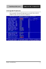
Page 49: ...f Size CPU Card S B C 6 5 7 B H S B 6 5 7 I Chapter3 Award BIOS Setup 3 9 3 6 Integrated Peripherals By choosing the Integrated Peripherals from the INITIAL SETUP SCREEN menu the screen below is displayed ...

Page 50: ...f Size CPU Card S B C 6 5 7 B H S B 6 5 7 I Chapter3 Award BIOS Setup 3 10 3 7 Power Management Setup By choosing the Power Management Setup from the INITIAL SETUP SCREEN menu the screen below is displayed ...

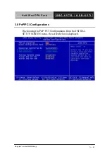
Page 51: ...f Size CPU Card S B C 6 5 7 B H S B 6 5 7 I Chapter3 Award BIOS Setup 3 11 3 8 PnP PCI Configurations By choosing the PnP PCI Configurations from the INITIAL SETUP SCREEN menu the screen below is displayed ...

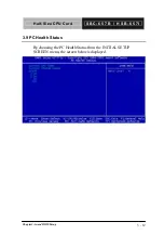
Page 52: ...Half Size CPU Card S B C 6 5 7 B H S B 6 5 7 I Chapter3 Award BIOS Setup 3 12 3 9 PC Health Status By choosing the PC Health Status from the INITIAL SETUP SCREEN menu the screen below is displayed ...

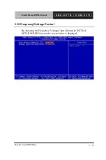
Page 53: ...ze CPU Card S B C 6 5 7 B H S B 6 5 7 I Chapter3 Award BIOS Setup 3 13 3 10 Frequency Voltage Control By choosing the Frequency Voltage Control from the INITIAL SETUP SCREEN menu the screen below is displayed ...

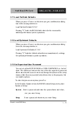
Page 54: ...ssing Y loads the default values that are manufacturer s settings for optimal performance system operations 3 13 Set Supervisor User Password You can set either SUPERVISOR or USER PASSWORD or both of them The difference between the two is that the supervisor password allows unrestricted access to enter and change the options of the setup menus while the user password only allows entry to the progr...

Page 55: ...ion and press Enter the values entered in the setup utilities will be recorded in the chipset s CMOS memory The microprocessor will check this every time you turnon your system and compare this to what it finds as it checks the system This record is required for the system to operate 3 15 Exit Without Saving Selecting this option and pressing Enter allows you to exit the Setup program without reco...

Page 56: ...Half Size CPU Card S B C 6 5 7 B H S B 6 5 7 I Chapter 4 Driver Installation 4 1 Driver Installation Chapter 4 ...

Page 57: ... and utilities of your needs There are several installation ways depending on the driver package under different Operating System application Please follow the sequence below to install the drivers Step 1 Install System Driver Step 2 Install VGA Driver Step 3 Install LAN Driver For installation procedures of each driver you may refer to section 4 1 4 2 ...

Page 58: ...xe icon A driver installation screen will appear Notice take VGA driver installation under Windows 98 for example choose the corresponding folder depending on your OS 3 A driver installation screen will appear please follow the onscreen instructions to install the driver in sequence and click on the Next button Notice In some cases the system will ask you to insert Windows 98 CD ROM and key in its...

Page 59: ... Next button 4 Select Search for the best driver for your device Recommended and click on the Next button 5 Select Specify a location click on Have Disk button then key in the CD ROM path and specify component drivers and OS folders Then click on the Next button 6 The Wizard shows that Windows driver file search for the device Click on the Next button 7 The system will ask you to insert Windows 98...

Page 60: ...Half Size CPU Card S B C 6 5 7 B H S B 6 5 7 I Appendix A Programming the Watchdog Timer A 1 Programming the Watchdog Timer Appendix A ...

Page 61: ... IRQ10 3 IRQ11 4 IRQ15 If you decide to program the watchdog timer you must write data to I O port 443 hex The output data is a value timer You can write form 01 hex to FF hex while simultaneously setting it When you want to disable the watchdog timer your program should read a Hex value from I O port 80 hex The following procesude is a sample program for the watchdog timer n Type C DOS Debug ENTE...

Reviews: