background image

S u b C o m p a c t   B o a r d    

G E N E - Q M 7 7


Chapter 2 Quick Installation Guide

 2-2


2.1 Safety Precautions   


Always completely disconnect the power cord 
from your board whenever you are working on 
it. Do not make connections while the power is 
on, because a sudden rush of power can 
damage sensitive electronic components. 


Always ground yourself to remove any static 
charge before touching the board. Modern 
electronic devices are very sensitive to static 
electric charges. Use a grounding wrist strap at 
all times. Place all electronic components on a 
static-dissipative surface or in a static-shielded 
bag when they are not in the chassis 


Summary of Contents for GENE-QM77

Page 1: ...7 GENE QM77 Intel 3rd Generation CoreTM i7 i5 Mobile Processor 10 100 1000Base TX Ethernet 2 USB3 0 6 USB 2 0 4 COM 8 bit Digital I O 2 SATA 6 0Gb s Optional RAID 1 CFast 1 Mini Card LPC GENE QM77 Ma...

Page 2: ...this manual is intended to be accurate and reliable However the original manufacturer assumes no responsibility for its use or for any infringements upon the rights of third parties that may result fr...

Page 3: ...Intel and Core are trademarks of Intel Corporation Microsoft Windows is a registered trademark of Microsoft Corp ITE is a trademark of Integrated Technology Express Inc IBM PC AT PS 2 and VGA are tra...

Page 4: ...stalling your card please make sure that the following materials have been shipped 1 Cooler 1 DVD ROM for Manual in PDF Format and Drivers 1 GENE QM77 If any of these items should be missing or damage...

Page 5: ...2 7 2 5 List of Connectors 2 8 2 6 Setting Jumpers 2 10 2 7 LVDS Port 2 Operating VDD Selection JP2 2 11 2 8 LVDS Port 1 Backlight Inverter VCC Selection JP3 2 11 2 9 LVDS Port 2 Backlight Inverter VC...

Page 6: ...2 18 2 24 LVDS Port 2 Inverter Backlight Connector CN7 2 18 2 25 Audio I O Port Connector CN8 2 19 2 26 LVDS Port 1 Connector CN9 2 19 2 27 LVDS Port 2 Connector CN10 2 21 2 28 COM Port 2 Connector CN...

Page 7: ...2 45 DDR3 SODIMM Slot CN29 2 42 2 46 Mini Card Slot CN30 2 42 2 47 SATA Port 1 SATA1 2 44 2 48 SATA Port 2 SATA2 2 45 Chapter 3 AMI BIOS Setup 3 1 System Test and Initialization 3 2 3 2 AMI BIOS Setup...

Page 8: ...ignments B 5 Appendix C Mating Connector C 1 List of Mating Connectors and Cables C 2 Appendix D RAID AHCI Settings D 1 Setting RAID D 2 D 2 Setting AHCI D 9 Appendix E Electrical Specifications for I...

Page 9: ...SubCompact Board G E N E Q M 7 7 Chapter 1 General Information 1 1 General Chapter 1 Information...

Page 10: ...hernet four COM ports two USB3 0 and six USB2 0 the GENE QM77 meets the requirements of today s demanding applications Display requirements are met with an abundance of interfaces such as CRT DVI and...

Page 11: ...le Processor Intel QM77 HM76 204 pin DDR3 1066 1333 1600 MHz SODIMM x 1 Up to 8 GB Gigabit Ethernet x 2 CRT 18 24 bit Dual Channel LVDS LCD x 2 DVI x 1 2CH HD Audio SATA 6 0Gb s x 2 Optional RAID CFas...

Page 12: ...E 10 100 1000Base TX RJ 45 x 2 BIOS AMI BIOS 16MB SPI Flash Wake On LAN Yes Watchdog Timer Generates a time out system reset H W Status Monitoring Supports power supply voltages and temperature monito...

Page 13: ...rated Memory Shared system memory up to 512MB Resolution Up to 2048x1536 for CRT Up to 1920 x 1200 for LCD DVI DVI DVI x 1 I O ITE IT8728F Fintek F81216D Storage SATA 6 0Gb s x 2 CFast x 1 Serial Port...

Page 14: ...SubCompact Board G E N E Q M 7 7 Chapter 2 Quick Installation Guide 2 1 Quick Installation Guide Chapter 2...

Page 15: ...while the power is on because a sudden rush of power can damage sensitive electronic components Always ground yourself to remove any static charge before touching the board Modern electronic devices a...

Page 16: ...SubCompact Board G E N E Q M 7 7 Chapter 2 Quick Installation Guide 2 3 2 2 Location of Connectors and Jumpers Component Side Component Side...

Page 17: ...SubCompact Board G E N E Q M 7 7 Chapter 2 Quick Installation Guide 2 4 Solder Side Solder Side...

Page 18: ...SubCompact Board G E N E Q M 7 7 Chapter 2 Quick Installation Guide 2 5 2 3 Mechanical Drawing Component Side Component Side So...

Page 19: ...SubCompact Board G E N E Q M 7 7 Chapter 2 Quick Installation Guide 2 6 Solder Side Solder Side...

Page 20: ...tion JP2 LVDS Port 2 Operating VDD Selection JP3 LVDS Port 1 Backlight Inverter VCC Selection JP4 LVDS Port 2 Backlight Inverter VCC Selection JP5 LVDS Port 1 Operating VDD Selection JP6 LVDS Port 1 B...

Page 21: ...tion CN1 LVDS Port 1 Inverter Backlight Connector CN2 External 12V Input CN3 USB 2 0 Ports 7 and 8 CN4 USB 2 0 Ports 5 and 6 CN5 USB 2 0 Ports 3 and 4 CN6 External 5VSB Input CN7 LVDS Port 2 Inverter...

Page 22: ...5V Output for SATA HDD CN23 Realtek LAN RJ 45 Port CN24 Intel LAN RJ 45 Port CN25 USB Ports 1 and 2 CN26 VGA DVI Ports depend on hardware configuration CN27 COM Port 1 D SUB 9 CN28 CFast Slot CN29 DD...

Page 23: ...t them To close a jumper you connect the pins with the clip To open a jumper you remove the clip Sometimes a jumper will have three pins labeled 1 2 and 3 In this case you would connect either pins 1...

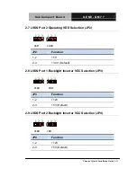
Page 24: ...ing VDD Selection JP2 1 2 3 1 2 3 5V 3 3V JP2 Function 1 2 5V 2 3 3 3V Default 2 8 LVDS Port 1 Backlight Inverter VCC Selection JP3 1 2 3 1 2 3 12V 5V JP3 Function 1 2 12V 2 3 5V Default 2 9 LVDS Port...

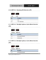
Page 25: ...2 3 1 2 3 5V 3 3V JP5 Function 1 2 5V 2 3 3 3V Default 2 11 LVDS Port 1 Backlight Lightness Control Mode Selection JP6 1 2 3 1 2 3 VR Mode PWM Mode JP6 Function 1 2 VR Mode Default 2 3 PWM Mode 2 12 L...

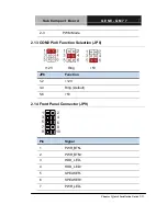
Page 26: ...tion Guide 2 13 2 3 PWM Mode 2 13 COM2 Pin8 Function Selection JP8 12V Ring 5V JP8 Function 1 2 12V 3 4 Ring Default 5 6 5V 2 14 Front Panel Connector JP9 1 2 3 4 5 6 7 8 9 10 Pin Signal 1 PWR_BTN 2 P...

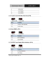
Page 27: ...ire Selection JP10 1 2 3 1 2 3 4 8 wire mode 5 wire mode JP10 Function 1 2 4 8 wire mode Default 2 3 5 wire mode 2 16 Clear CMOS JP11 1 2 3 1 2 3 Normal Clear CMOS JP11 Function 1 2 Normal Default 2 3...

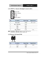
Page 28: ...5 1 BKL_CONTROL GND GND BKL_ENABLE Pin Pin Name Signal Type Signal Level 1 BKL_PWR PWR 5V 12V 2 BKL_CONTROL OUT 3 GND GND 4 GND GND 5 BKL_ENABLE OUT 5V Note LVDS1 BKL_PWR can be set to 5V or 12V by J...

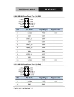
Page 29: ...0 USB7_D USB7_D GND GND Pin Pin Name Signal Type Signal Level 1 5VSB PWR 5V 2 GND GND 3 USB7_D DIFF 4 GND GND 5 USB7_D DIFF 6 USB8_D DIFF 7 GND GND 8 USB8_D DIFF 9 GND GND 10 5VSB PWR 5V 2 21 USB2 0 P...

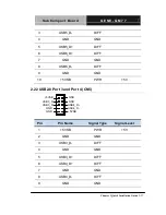
Page 30: ...F 6 USB6_D DIFF 7 GND GND 8 USB6_D DIFF 9 GND GND 10 5VSB PWR 5V 2 22 USB2 0 Port 3 and Port 4 CN5 GND GND USB4_D USB4_D 5VSB 5VSB 1 2 9 10 USB3_D USB3_D GND GND Pin Pin Name Signal Type Signal Level...

Page 31: ...Type Signal Level 1 PS_ON OUT 3 3V 2 GND GND 3 5VSB PWR 5V 2 24 LVDS Port 2 Inverter Backlight Connector CN7 BLK_PWR 2 3 4 5 1 BKL_CONTROL GND GND BKL_ENABLE Pin Pin Name Signal Type Signal Level 1 B...

Page 32: ...LINE_L_IN LINE_R_IN LEFT_OUT RIGHT_OUT 5V_AUDIO GND_AUDIO GND_AUDIO GND_AUDIO Pin Pin Name Signal Type Signal Level 1 MIC_L IN 2 MIC_R IN 3 GND_AUDIO GND 4 LINE_L_IN IN 5 LINE_R_IN IN 6 GND_AUDIO GND...

Page 33: ...WR PWR 3 3V 5V 4 GND GND 5 LVDS_A_CLK DIFF 6 LVDS_A_CLK DIFF 7 LCD_PWR PWR 3 3V 5V 8 GND GND 9 LVDS_DA0 DIFF 10 LVDS_DA0 DIFF 11 LVDS_DA1 DIFF 12 LVDS_DA1 DIFF 13 LVDS_DA2 DIFF 14 LVDS_DA2 DIFF 15 LVD...

Page 34: ...PWR 3 3V 5V 28 GND GND 29 LVDS_B_CLK DIFF 30 LVDS_B_CLK DIFF Note LVDS1 LCD_PWR can be set to 3 3V or 5V by JP5 2 27 LVDS Port 2 Connector CN10 PIN 1 PIN 2 PIN 30 PIN 29 Pin Pin Name Signal Type Sign...

Page 35: ...A2 DIFF 14 LVDS_DA2 DIFF 15 LVDS_DA3 DIFF 16 LVDS_DA3 DIFF 17 DDC_DATA I O 3 3V 18 DDC_CLK I O 3 3V 19 LVDS_DB0 DIFF 20 LVDS_DB0 DIFF 21 LVDS_DB1 DIFF 22 LVDS_DB1 DIFF 23 LVDS_DB2 DIFF 24 LVDS_DB2 DIF...

Page 36: ...1 2 3 4 5 6 7 8 9 2 28 COM Port 2 Connector CN11 RS 232 Pin Pin Name Signal Type Signal Level 1 DCD IN 2 DSR IN 3 RX IN 4 RTS OUT 9V 5 TX OUT 9V 6 CTS IN 7 DTR OUT 9V 8 RI 5V 12V IN PWR 5V 12V 9 GND...

Page 37: ...X OUT 5V 6 NC 7 RS422_RX IN 8 NC 5V 12V PWR 5V 12V 9 GND GND RS 485 Pin Pin Name Signal Type Signal Level 1 RS485_D I O 5V 2 NC 3 NC 4 NC 5 RS485_D I O 5V 6 NC 7 NC 8 NC 5V 12V PWR 5V 12V 9 GND GND No...

Page 38: ...0 DIO1 DIO2 DIO3 N C N C N C N C DIO7 DIO6 DIO5 DIO4 STROBE 1 2 25 26 1 2 25 26 AFD ERROR PRINT SLIN GND GND GND GND GND GND GND GND N C PD0 PD1 PD2 PD3 PD4 PD5 PD6 PD7 ACK BUSY PE SLCT LPT Mode DIO M...

Page 39: ...D 23 PE IN 24 GND GND 25 SLCT IN 26 NC Note LPT Digital IO can be set by BIOS setting Default is LPT Function DIO Mode N C N C N C N C N C GND GND GND GND GND GND GND GND N C DIO0 DIO1 DIO2 DIO3 N C N...

Page 40: ...27 Pin Pin Name Signal Type Signal Level 1 NC 2 NC 3 DIO0 I O 5V 4 NC 5 DIO1 I O 5V 6 NC 7 DIO2 I O 5V 8 NC 9 DIO3 I O 5V 10 GND GND 11 NC 12 GND GND 13 NC 14 GND GND 15 NC 16 GND GND 17 NC 18 GND GN...

Page 41: ...Bit 0 of 0xA06 Port 2 DIO1 5 Bit 1 of 0xA06 Port 3 DIO2 7 Bit 2 of 0xA06 Port 4 DIO3 9 Bit 3 of 0xA06 Port 5 DIO4 25 Bit 0 of 0xA07 Port 6 DIO5 23 Bit 1 of 0xA07 Port 7 DIO6 21 Bit 2 of 0xA07 Port 8 D...

Page 42: ...E LRESET LDRQ0 LDRQ1 SERIRQ GND LCLK 3 3V 6 CTS IN 7 DTR OUT 9V 8 RI IN 9 GND GND 2 31 LPC Port Connector CN14 Pin Pin Name Signal Type Signal Level 1 LAD0 I O 3 3V 2 LAD1 I O 3 3V 3 LAD2 I O 3 3V 4 L...

Page 43: ...RQ I O 3 3V 2 32 COM Port 4 Connector CN15 Pin Pin Name Signal Type Signal Level 1 DCD IN 2 DSR IN 3 RX IN 4 RTS OUT 9V 5 TX OUT 9V 6 CTS IN 7 DTR OUT 9V 8 RI IN 9 GND GND 2 33 UIM Card Module CN16 UI...

Page 44: ...el 1 UIM_PWR PWR 2 UIM_RST IN 3 UIM_CLK IN 4 GND GND 5 UIM_VPP PWR 6 UIM_DATA I O 2 34 PS 2 Keyboard Mouse Combo Port Connector CN17 KB_CLK KB_DATA 1 5 6 2 MS_DATA 5VSB GND MS_CLK Pin Pin Name Signal...

Page 45: ...FT SENSE RIGHT SENSE GND TOP BOTTOM LEFT RIGHT NC NC NC NC GND UL Y UR H LL L LR X SENSE S NC NC NC 8 Wires 4 Wires 5 Wires 2 35 5VSB Output w SMBus CN18 Pin Pin Name Signal Type Signal Level 1 SMB_DA...

Page 46: ...ENSE GND TOP BOTTOM LEFT RIGHT NC NC NC NC GND UL Y UR H LL L LR X SENSE S NC NC NC 8 Wires 4 Wires 5 Wires 4 LEFT EXCITE IN 5 RIGHT EXCITE IN 6 TOP SENSE IN 7 BOTTOM SENSE IN 8 LEFT SENSE IN 9 RIGHT...

Page 47: ...LEFT RIGHT NC NC NC NC GND UL Y UR H LL L LR X SENSE S NC NC NC 4 Wires 5 Wires 5 wire Pin Pin Name Signal Type Signal Level 1 GND GND 2 UL Y IN 3 UR H IN 4 LL L IN 5 LR X IN 6 SENSE S IN 7 NC 8 NC 9...

Page 48: ...ignal Level 1 GND GND 2 FAN_POWER PWR 5V 3 FAN_TAC IN 2 38 5V Output for SATA HDD CN22 5V GND Pin Pin Name Signal Type Signal Level 1 5V PWR 5V 2 GND GND 2 39 Realtek LAN RJ 45 Port CN23 1 ACT LINK LE...

Page 49: ...ation Guide 2 36 5 MDI2 DIFF 6 MDI1 DIFF 7 MDI3 DIFF 8 MDI3 DIFF 2 40 Intel LAN RJ 45 Port CN24 1 ACT LINK LED SPEED LED 8 Pin Pin Name Signal Type Signal Level 1 MDI0 DIFF 2 MDI0 DIFF 3 MDI1 DIFF 4 M...

Page 50: ...2 Port 1 11 12 13 1 2 3 4 14 15 16 17 18 5 6 7 8 9 Pin Pin Name Signal Type Signal Level 1 5VSB PWR 5V 2 USB1_D DIFF 3 USB1_D DIFF 4 GND GND 5 USB1_SSRX DIFF 6 USB1_SSRX DIFF 7 GND GND 8 USB1_SSTX DI...

Page 51: ...FF 18 USB2_SSTX DIFF 2 42 VGA DVI Ports depend on hardware configuration CN26 1 1 9 C1 C5 C2 C3 C4 17 8 16 24 6 10 11 15 5 VGA Pin Pin Name Signal Type Signal Level 1 RED OUT 2 GREEN OUT 3 BLUE OUT 4...

Page 52: ...I O 5V DVI Pin Pin Name Signal Type Signal Level 1 TMDS_DAT2 DIFF 2 TMDS_DAT2 DIFF 3 GND GND 4 VGA_DDC_CLK I O 5 VGA_DDC _DATA I O 6 DVI_DDC_CLK I O 5V 7 DVI_DDC_DATA I O 5V 8 VSYNC OUT 9 TMDS_DAT1 D...

Page 53: ...DAT0 DIFF 19 GND GND 20 NC 21 NC 22 GND GND 23 TMDS_CLK DIFF 24 TMDS_CLK DIFF C1 RED OUT C2 GREEN OUT C3 BLUE OUT C4 HSYNC OUT C5 GND_ANALOG GND 2 43 COM Port 1 D SUB 9 CN27 1 5 6 9 Pin Pin Name Signa...

Page 54: ...RTS OUT 9V 8 CTS IN 9 RI IN 2 44 CFast Slot CN28 Pin Pin Name Signal Type Signal Level S1 GND GND S2 SATA_TX DIFF S3 SATA_TX DIFF S4 GND GND S5 SATA_RX DIFF S6 SATA_RX DIFF S7 GND GND PC1 NC PC2 GND...

Page 55: ...3 3V PC15 GND GND PC16 GND GND PC17 NC 2 45 DDR3 SODIMM Slot CN29 Standard specification 2 46 Mini Card Slot CN30 Pin Pin Name Signal Type Signal Level 1 PCIE_WAKE IN 2 3 3VSB PWR 3 3V 3 NC 4 GND GND...

Page 56: ...GND GND 16 UIM_VPP PWR 17 NC 18 GND GND 19 NC 20 W_DISABLE OUT 3 3V 21 GND GND 22 PCIE_RST OUT 3 3V 23 PCIE_RX DIFF 24 3 3VSB PWR 3 3V 25 PCIE_RX DIFF 26 GND GND 27 GND GND 28 1 5V PWR 1 5V 29 GND GN...

Page 57: ...37 GND GND 38 USB_D DIFF 39 3 3VSB PWR 3 3V 40 GND GND 41 3 3VSB PWR 3 3V 42 NC 43 GND GND 44 NC 45 NC 46 NC 47 NC 48 1 5V PWR 1 5V 49 NC 50 GND GND 51 NC 52 3 3VSB PWR 3 3V 2 47 SATA Port 1 SATA1 Pi...

Page 58: ...nstallation Guide 2 45 3 SATA_TX DIFF 4 GND GND 5 SATA_RX DIFF 6 SATA_RX DIFF 7 GND GND 2 48 SATA Port 2 SATA2 Pin 1 Pin 7 Pin Pin Name Signal Type Signal Level 1 GND GND 2 SATA_TX DIFF 3 SATA_TX DIFF...

Page 59: ...act Board G E N E Q M 7 7 Chapter 2 Quick Installation Guide 2 46 Below Table for China RoHS Requirements AAEON Main Board Daughter Board Backplane Pb Hg Cd Cr VI PBB PBDE O SJ T 11363 2006 X SJ T 113...

Page 60: ...SubCompact Board G E N E Q M 7 7 Chapter 3 AMI BIOS Setup 3 1 AMI Chapter 3 BIOS Setup...

Page 61: ...n against the values stored in the CMOS memory If they do not match the program outputs an error message You will then need to run the BIOS setup program to set the configuration information in memory...

Page 62: ...it retains the Setup information when the power is turned off Entering Setup Power on the computer and press Del or F2 immediately This will allow you to enter Setup Main Set the date use tab to swit...

Page 63: ...SubCompact Board G E N E Q M 7 7 Chapter 4 Driver Installation 4 1 0BDriver Installation Chapter 4...

Page 64: ...not please follow the sequence below to install the drivers Follow the sequence below to install the drivers Step 1 Install Chipset Driver Step 2 Install VGA Driver Step 3 Install LAN Driver Realtek L...

Page 65: ...ly Step 2 Install VGA Driver 1 Click on the STEP2 VGA folder and select the OS folder your system is 2 Double click on the Setup exe file located in each OS folder 3 Follow the instructions that the w...

Page 66: ...The system will help you install the driver automatically Step 5 Install Audio Driver 1 Click on the STEP5 AUDIO folder and select the OS folder your system is 2 Double click on the Setup exe file loc...

Page 67: ...l the driver automatically Step 9 Install Touch Driver 1 Click on the STEP9 TOUCH folder and select the OS folder your system is 2 Double click on the Setup exe file located in each OS folder 3 Follow...

Page 68: ...SubCompact Board G E N E Q M 7 7 Appendix A Programming the Watchdog Timer A 1 Programming the Appendix A Watchdog Timer...

Page 69: ...tial watchdog timer program is also attached based on which you can develop customized program to fit your application Configuring Sequence Description After the hardware reset or power on reset the I...

Page 70: ...Wait for Key state To ensure the initial state of the key check logic it is necessary to perform four write operations to the Special Address port 2EH Two different enter keys are provided to select c...

Page 71: ...he Watchdog Timer A 4 WatchDog Timer Configuration Registers Configure Control Index 02h This register is write only Its values are not sticky that is to say a hardware reset will automatically clear...

Page 72: ...M 7 7 Appendix A Programming the Watchdog Timer A 5 WatchDog Timer Control Register Index 71h Default 00h WatchDog Timer Configuration Register Index 72h Default 00h WatchDog Timer Time out Value Regi...

Page 73: ...ODE Main CALL Enter_Configuration_mode CALL Check_Chip mov cl 7 call Set_Logic_Device time setting mov cl 10 10 Sec dec al Watch_Dog_Setting Timer setting mov al cl mov cl 73h call Superio_Set_Reg Cle...

Page 74: ...ce Initial_OK CALL Exit_Configuration_mode MOV AH 4Ch INT 21h Enter_Configuration_Mode PROC NEAR MOV SI WORD PTR CS Offset Cfg_Port MOV DX 02Eh MOV CX 04h Init_1 MOV AL BYTE PTR CS SI OUT DX AL INC SI...

Page 75: ...n_Mode ENDP Check_Chip PROC NEAR MOV AL 20h CALL Read_Configuration_Data CMP AL 87h JNE Not_Initial MOV AL 21h CALL Read_Configuration_Data CMP AL 12h JNE Not_Initial Need_Initial STC RET Not_Initial...

Page 76: ...Write_Configuration_Data PROC NEAR MOV DX WORD PTR CS Cfg_Port 04h OUT DX AL XCHG AL AH MOV DX WORD PTR CS Cfg_Port 06h OUT DX AL RET Write_Configuration_Data ENDP Superio_Set_Reg proc near push ax MO...

Page 77: ...cx xchg al cl mov cl 07h call Superio_Set_Reg pop cx pop ax ret Set_Logic_Device endp Select 02Eh Index Port 02Fh Data Port Cfg_Port DB 087h 001h 055h 055h DW 02Eh 02Fh END Main Note Interrupt level...

Page 78: ...SubCompact Board G E N E Q M 7 7 Appendix B I O Information B 1 I O Information Appendix B...

Page 79: ...SubCompact Board G E N E Q M 7 7 Appendix B I O Information B 2 B 1 I O Address Map...

Page 80: ...SubCompact Board G E N E Q M 7 7 Appendix B I O Information B 3...

Page 81: ...SubCompact Board G E N E Q M 7 7 Appendix B I O Information B 4 B 2 Memory Address Map...

Page 82: ...SubCompact Board G E N E Q M 7 7 Appendix B I O Information B 5 B 3 IRQ Mapping Chart B 4 DMA Channel Assignments...

Page 83: ...SubCompact Board G E N E Q M 7 7 Appendix C Mating Connector C 1 Mating Connector Appendix C...

Page 84: ...ort 5 6 Connector Molex 51110 1050 USB Cable 1709100201 CN5 USB Port 3 4 Connector Molex 51110 1050 USB Cable 1709100201 CN6 External 5VSB Power Input and PS_ON JST XHP 3 ATX Cable 170220020B CN7 LVDS...

Page 85: ...N16 UIM Connector Molex 51021 0600 N A N A CN17 P S2 KB MS Connector JST PHDR 06VS P S2 KB MS Cable 1700060152 CN18 External AUX Power and PS_ON JST PHR 6 N A N A CN19 Touch Screen Connector JST SHR 9...

Page 86: ...SubCompact Board G E N E Q M 7 7 Appendix D RAID AHCI Settings D 1 RAID AHCI Appendix D Settings...

Page 87: ...ings D 2 D 1 Setting RAID OS installation to SETUP RAID Mode Step 1 Extract the f6fly x86 zip from Driver CD Step7 RAID AHCI WinXP_32 and copy below files to diskette Step 2 Connect the USB Floppy dri...

Page 88: ...E N E Q M 7 7 Appendix D RAID AHCI Settings D 3 Step 3 Configure SATA Controller to RAID mode in BIOS SETUP Menu Advanced SATA Configuration SATA Mode RAID Mode Step 4 Configure DVD CD ROM drive as th...

Page 89: ...SubCompact Board G E N E Q M 7 7 Appendix D RAID AHCI Settings D 4 Step 5 Save changes and exit BIOS SETUP Step 6 Press CTRL I to enter RAID Configuration Utility...

Page 90: ...SubCompact Board G E N E Q M 7 7 Appendix D RAID AHCI Settings D 5 Step 7 Choose 1 Create RAID Volume Step 8 Configure RAID parameters for the system...

Page 91: ...SubCompact Board G E N E Q M 7 7 Appendix D RAID AHCI Settings D 6 Step 9 Choose Create Volume and confirmed in next warning message...

Page 92: ...G E N E Q M 7 7 Appendix D RAID AHCI Settings D 7 Step 10 Exit RAID Configuration Utility and Reboot to DVD CD ROM device to install OS Step 11 Press F6 to install RAID driver Step 12 Press S to inst...

Page 93: ...N E Q M 7 7 Appendix D RAID AHCI Settings D 8 Step 13 Choose Intel R Mobile Express Chipset SATA RAID Controller Step 14 It will show the model you selected and then press ENTER Windows Setup will co...

Page 94: ...ings D 9 D 2 Setting AHCI OS installation to SETUP AHCI Mode Step 1 Extract the f6fly x86 zip from Driver CD Step7 RAID AHCI WinXP_32 and copy below files to diskette Step 2 Connect the USB Floppy dri...

Page 95: ...N E Q M 7 7 Appendix D RAID AHCI Settings D 10 Step 3 Configure SATA Controller to RAID mode in BIOS SETUP Menu Advanced SATA Configuration SATA Mode AHCI Mode Step 4 Configure DVD CD ROM drive as th...

Page 96: ...SubCompact Board G E N E Q M 7 7 Appendix D RAID AHCI Settings D 11 Step 5 Save changes and exit BIOS SETUP Step 6 Boot to DVD CD ROM device to install OS Step 7 Press F6 to install AHCI driver...

Page 97: ...SubCompact Board G E N E Q M 7 7 Appendix D RAID AHCI Settings D 12 Step 8 Press S to install AHCI driver Step 9 Choose Intel R 7 Series Chipset Family SATA AHCI Controller...

Page 98: ...SubCompact Board G E N E Q M 7 7 Appendix D RAID AHCI Settings D 13 Step 10 It will show the model you selected and then press ENTER Windows Setup will continue to install OS...

Page 99: ...SubCompact Board G E N E Q M 7 7 Appendix E Electrical Specifications for I O Ports E 1 Electrical Specifications Appendix E for I O Ports...

Page 100: ...and 8 CN3 5V USB 2 0 Ports 5 and 6 CN4 5V 5V 0 5A per channel USB 2 0 Ports 3 and 4 CN5 5V USB Ports 1 and 2 CN25 VCC 5V 1A per channel Audio I O Port CN8 5V 5V 1A LVDS Port 1 CN9 VCC 3 3V 1A or 5V 1A...

Page 101: ...bCompact Board G E N E Q M 7 7 Appendix E Electrical Specifications for I O Ports E 3 CFast Slot CN28 3 3V 3 3V 0 5A Mini Card Slot CN30 3 3VSB 1 5V 3 3V 1 1A 1 5V 0 375A LPC Port CN14 3 3VCC 3 3V 0 5...

Reviews: