Chapter 2 – Hardware Information
13
3.5
” S
ub
co
mp
act
Bo
ard
G
ENE
-HD05
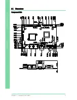
2.4 List of Connectors
Please refer to the table below for all of the board‟s connectors that you can configure
for your application
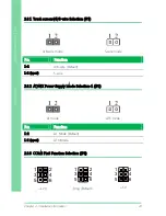
Note: If CN4 (power input for 5VSB input) is not used, please short JP9 (set pin1 and
pin2 to short).
If CN4 (power input for 5VSB input) is used, please leave JP9 open (set pin1 and pin2
to open).
Label
Function
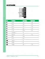
CN1
LPC Port
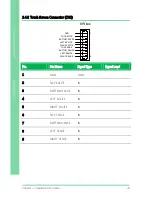
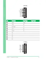
CN2
Touch Screen Connector
CN3
CPU FAN
CN4
Ex5VSB Input
CN5
Ex12V Input
CN6
Front Panel Connector
CN7
Digital IO Port
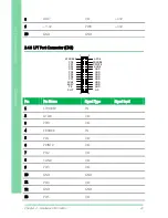
CN8
LPT Port
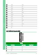
CN9
COM Port 2
CN10
COM Port 3
CN11
COM Port 4
CN12
USB 2.0 Ports 7
CN13
USB 2.0 Ports 8
CN14
USB 2.0 Ports 5
CN15
USB 2.0 Ports 6
CN16
USB 2.0 Ports 3
Summary of Contents for GENE-HD05
Page 1: ...Last Updated November 10 2015 GENE HD05 3 5 Subcompact Board User s Manual 4th Ed...
Page 15: ...3 5 Subcompact Board GENE HD05 Chapter 1 Chapter 1 Product Specifications...
Page 18: ...3 5 Subcompact Board GENE HD05 Chapter 2 Chapter 2 Hardware Information...
Page 20: ...Chapter 2 Hardware Information 6 3 5 Subcompact Board GENE HD05 Solder Side Solder Side...
Page 22: ...Chapter 2 Hardware Information 8 3 5 Subcompact Board GENE HD05 Solder Side Solder Side...
Page 56: ...3 5 Subcompact Board GENE HD05 Chapter 3 Chapter 3 AMI BIOS Setup...
Page 63: ...Chapter 3 AMI BIOS Setup 49 3 5 Subcompact Board GENE HD05 3 4 2 Advanced CPU Configuration...
Page 71: ...Chapter 3 AMI BIOS Setup 57 3 5 Subcompact Board GENE HD05 RS485 RS232 422 485 switch...
Page 87: ...3 5 Subcompact Board GENE HD05 Chapter 4 Chapter 4 Drivers Installation...
Page 90: ...3 5 Subcompact Board GENE HD05 Appendix A Appendix A Watchdog Timer Programming...
Page 93: ...Appendix A Watchdog Timer Programming 79 3 5 Subcompact Board GENE HD05...
Page 96: ...3 5 Subcompact Board GENE HD05 Appendix B Appendix B I O Information...
Page 97: ...Appendix B I O Information 83 3 5 Subcompact Board GENE HD05 B 1 I O Address Map...
Page 98: ...Appendix B I O Information 84 3 5 Subcompact Board GENE HD05...
Page 99: ...Appendix B I O Information 85 3 5 Subcompact Board GENE HD05 B 2 First MB Memory Address Map...
Page 100: ...Appendix B I O Information 86 3 5 Subcompact Board GENE HD05 B 3 IRQ Mapping Chart...
Page 101: ...Appendix B I O Information 87 3 5 Subcompact Board GENE HD05 B 4 DMA Channel Assignments...
Page 102: ...3 5 Subcompact Board GENE HD05 Appendix C Appendix C Mating Connectors...
Page 105: ...3 5 Subcompact Board GENE HD05 Appendix D Appendix D AHCI Settings...
Page 108: ...Appendix D AHCI Settings 94 3 5 Subcompact Board GENE HD05 Step 5 Press F6 Step 6 Choose S...
Page 110: ...3 5 Subcompact Board GENE HD05 Appendix E Appendix E Electrical Specifications for I O Ports...


