background image

E P I C   B o a r d  

E P I C - H D 0 7


          i 

Copyright Notice 


This document is copyrighted, 2012. All rights are reserved. The 
original manufacturer reserves the right to make improvements to the 
products described in this manual at any time without notice. 

No part of this manual may be reproduced, copied, translated, or 
transmitted in any form or by any means without the prior written 
permission of the original manufacturer. Information provided in this 
manual is intended to be accurate and reliable. However, the original 
manufacturer assumes no responsibility for its use, or for any in-
fringements upon the rights of third parties that may result from its 
use. 

The material in this document is for product information only and is 
subject to change without notice. While reasonable efforts have been 
made in the preparation of this document to assure its accuracy, 
AAEON assumes no liabilities resulting from errors or omissions in 
this document, or from the use of the information contained herein. 

AAEON reserves the right to make changes in the product design 
without notice to its users. 

All manuals and user guides at all-guides.com

Summary of Contents for EPIC-HD07

Page 1: ...T44R T40R Processor Onboard DDR3 1066 1333 SODIMM 18 24 bit Single Dual channel LVDS LCD 8 USB 2 0 6 COM 1 SATA 1 mSATA 2 GbE PCI 104 Mini Card EPIC HD07 Manual Rev A 2nd Ed May 2012 All manuals and...

Page 2: ...be accurate and reliable However the original manufacturer assumes no responsibility for its use or for any in fringements upon the rights of third parties that may result from its use The material i...

Page 3: ...anced Micro Devices Microsoft Windows is a registered trademark of Microsoft Corp ITE is a trademark of Integrated Technology Express Inc IBM PC AT PS 2 and VGA are trademarks of International Busines...

Page 4: ...that the following materials have been shipped 1709070500 SATA Cable 1702150155 SATA Power Cable 9657666600 Jumper Cap Product DVD EPIC HD07 If any of these items are missing or damaged please contact...

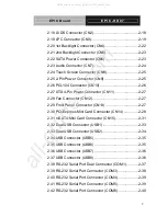
Page 5: ...6 Setting Jumpers 2 11 2 7 AT ATX Selection JP1 2 12 2 8 COM2 Ring 5V 12V Selection JP2 2 12 2 9 2nd LVDS External Backlight Control JP3 2 12 2 10 LCD Panel Voltage Selection JP4 2 13 2 11 LCD Backlig...

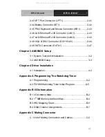
Page 6: ...2 29 Front Panel Connector CN13 2 27 2 30 PCI Express Mini Card Connector CN14 2 28 2 31 mSATA Mini Card Connector CN15 2 31 2 32 Dual USB Connector USB1 2 33 2 33 Dual USB Connector USB2 2 34 2 34 US...

Page 7: ...pter 3 AMI BIOS Setup 3 1 System Test and Initialization 3 2 3 2 AMI BIOS Setup 3 3 Chapter 4 Driver Installation 4 1 Installation 4 3 Appendix A Programming The Watchdog Timer A 1 Programming A 2 A 2...

Page 8: ...E P I C H D 0 7 vii Appendix D AHCI Setting D 1 Setting AHCI D 2 Appendix E Electrical Specifications for I O Ports E 1 Electrical Specifications for I O Ports E 2 All manuals and user guides at all...

Page 9: ...EPIC Board E P I C H D 0 7 Chapter 1 General Information 1 1 General Chapter 1 Information All manuals and user guides at all guides com...

Page 10: ...hieve an excellent performance In addition EPIC HD07 deploys Realtek 8111E Ethernet chip to feature two RJ 45 ports onboard to display the transcendent performance of network connections The display c...

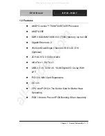
Page 11: ...Ethernet x 2 18 24 bit Dual Single Channel LVDS LCD DVI Optional 2CH AC97 2 3 Codec Audio mSATA x 1 SATA x 1 USB 2 0 x 8 COM x 6 16 bit Digital I O Co lay With LPT PCI 104 Mini Card Expansions DC 12V...

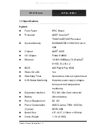
Page 12: ...TX Realtek 8111E RJ 45 x 2 BIOS AMI Plug Play BIOS Wake On LAN Yes Watchdog Timer Generates a time out system reset H W Status Monitoring Supports power supply voltages fan speed and temperature moni...

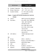
Page 13: ...ted Resolutions Up to 2560 x 1600 T56N 18W 1920 x 1200 T44R T40R 9W 5 5W for CRT Up to 1920x1200 for DVI Up to 1400 x 1050 for single channel LVDS Up to 1920 x 1200 for dual channel LVDS LCD Interface...

Page 14: ...EPIC Board E P I C H D 0 7 Chapter 1 General Information 1 6 Audio Line in Line out Mic in Touch Screen Supports 4 5 wire resistive touch screen optional All manuals and user guides at all guides com...

Page 15: ...EPIC Board E P I C H D 0 7 Chapter 2 Quick Installation Guide 2 1 Quick Installation Chapter 2 Guide All manuals and user guides at all guides com...

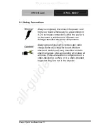
Page 16: ...rush of power can damage sensitive electronic components Always ground yourself to remove any static charge before touching the board Modern electronic devices are very sensitive to static electric c...

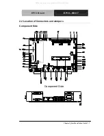
Page 17: ...EPIC Board E P I C H D 0 7 Chapter 2 Quick Installation Guide 2 3 2 2 Location of Connectors and Jumpers Component Side Component Side All manuals and user guides at all guides com...

Page 18: ...EPIC Board E P I C H D 0 7 Solder Side Chapter 2 Quick Installation Guide 2 4 All manuals and user guides at all guides com...

Page 19: ...EPIC Board E P I C H D 0 7 Chapter 2 Quick Installation Guide 2 5 2 3 Mechanical Drawing Component Side Component Side All manuals and user guides at all guides com...

Page 20: ...EPIC Board E P I C H D 0 7 Chapter 2 Quick Installation Guide 2 6 Solder Side All manuals and user guides at all guides com...

Page 21: ...E P I C H D 0 7 Chapter 2 Quick Installation Guide 2 7 Heatsink 3 0 a a a a b b b b b b c c b b b b 3 0 3 0 e e e e e e Thermal Block and Pad All manuals and user guides at all guides com a l l g u i...

Page 22: ...each of the board s jumpers Label Function JP1 AT ATX Function Selection JP2 COM2 Ring 5V 12V Selection JP3 2nd LVDS External Backlight Control JP4 LCD Panel Voltage Selection JP5 LCD Backlight Contr...

Page 23: ...3 LPC Connector CN4 1 st Backlight Connector CN5 2 nd Backlight Connector CN6 SATA Power Connector CN7 Audio Connector CN8 Touch Panel Connector CN9 2 Pin Power Connector optional CN10 PCI 104 Connect...

Page 24: ...Port Connector COM2 Dual Port 2 COM2 RS 232 422 485 Serial Port Connector COM3 COM3 RS 232 Serial Port Connector COM4 COM4 RS 232 Serial Port Connector COM5 COM5 RS 232 Serial Port Connector COM6 COM...

Page 25: ...ou connect the pins with the clip To open a jumper you remove the clip Sometimes a jumper will have three pins labeled 1 2 and 3 In this case you would connect either pins 1 and 2 or 2 and 3 1 2 3 Ope...

Page 26: ...OFF Default AT ON 2 8 COM2 Ring 5V 12V Selection JP2 12V 5V RI2 JP2 Function 1 2 12V 3 4 RI2 _SEL Default 5 6 5V 2 9 2nd LVDS External Backlight Control JP3 1 2 3 1 2 3 Backlight up Backlight down JP3...

Page 27: ...0 LCD Panel Voltage Selection JP4 LVDS1 5V JP4 Function 1 3 5V 3 5 3 3V Default LVDS2 3 3V 5V JP4 Function 2 4 5V 4 6 3 3V Default 2 11 LCD Backlight Control Selection JP5 LVDS1 1 5 6 2 3 4 1 5 6 2 3...

Page 28: ...oltage Mode 3 5 PWM Mode Default LVDS2 1 5 6 2 3 4 1 5 6 2 3 4 Voltage mode PWM mode JP5 Function 2 4 Voltage Mode 4 6 PWM Mode Default 2 12 LCD Backlight Voltage Selection JP6 LVDS1 5V 12V JP6 Functi...

Page 29: ...2V Default 2 13 Clear CMOS JP7 1 2 3 1 2 3 Normal Clear CMOS JP7 Function 1 2 Protected Default 2 3 Clear 2 14 DDR3 DDR3L Voltage Control JP8 DDR3 DDR3L JP8 Function OFF DDR3 Default ON DDR3L 2 15 PC...

Page 30: ...6 Touch Screen Connector Selection JP10 5 Wire 4 Wire JP10 Function ON 4 Wire Default OFF 5 Wire 2 17 LVDS Connector CN1 Pin Pin Name Signal Type Signal Level 1 LVDS_BKLEN OUT 2 LVDS_BKLCTL OUT 3 LCD_...

Page 31: ...UT 11 LVDS_TXL1 OUT 12 LVDS_TXL1 OUT 13 LVDS_TXL2 OUT 14 LVDS_TXL2 OUT 15 LVDS_TXL3 OUT 16 LVDS_TXL3 OUT 17 LVDS_DDCPDATA I O 3 3V 18 LVDS_DDCPCLK I O 3 3V 19 N C 20 N C 21 N C 22 N C 23 N C 24 N C 25...

Page 32: ..._BKLEN OUT 2 LVDS_BKLCTL OUT 3 LCD_PWR PWR 3 3V 5V 4 GND GND 5 LVDS_TXLCLK OUT 6 LVDS_TXLCLK OUT 7 LCD_PWR PWR 3 3V 5V 8 GND GND 9 LVDS_TXL0 OUT 10 LVDS_TXL0 OUT 11 LVDS_TXL1 OUT 12 LVDS_TXL1 OUT 13 L...

Page 33: ...3V 19 LVDS_TXU0 OUT 20 LVDS_TXU0 OUT 21 LVDS_TXU1 OUT 22 LVDS_TXU1 OUT 23 LVDS_TXU2 OUT 24 LVDS_TXU2 OUT 25 LVDS_TXU3 OUT 26 LVDS_TXU3 OUT 27 LCD_PWR PWR 3 3V 5V 28 GND GND 29 LVDS_TXUCLK OUT 30 LVDS_...

Page 34: ...3 I O 5 3 3V PWR 3 3V 6 LFRAME OUT 7 LPC_RST OUT 8 GND GND 9 LPC_CLK33 OUT 10 LDRQ 0 OUT 11 LDRQ 1 OUT 12 SERIRQ OUT DIO Mode DIO co lay with LPT Pin Pin Name Signal type Signal Level 1 GPIO15 I O 2 G...

Page 35: ...ND 13 GPIO5 I O 14 GND GND 15 GPIO6 I O 16 GND GND 17 GPIO7 I O 18 GPIO6 I O 19 GPIO10 I O 20 GND GND 21 GPIO9 I O 22 GND GND 23 GPIO8 I O 24 GND GND 25 N C 26 N C NO Pin Name Pin Number Access Addres...

Page 36: ...21 11 GPIO10 19 12 GPIO11 8 13 GPIO12 6 14 GPIO13 4 15 GPIO14 2 16 GPIO15 1 2 20 1st Backlight Connector CN4 Pin Pin Name Signal Type Signal Level 1 LVDS Backlight PWR OUT 2 LVDS Backlight control OU...

Page 37: ...ector CN5 Pin Pin Name Signal Type Signal Level 1 LVDS Backlight PWR OUT 2 LVDS Backlight control OUT 3 GND GND 4 GND GND 5 LVDS Backlight Enable OUT 2 22 SATA Power Connector CN6 Pin Pin Name Signal...

Page 38: ...2 24 2 23 Audio Connector CN7 Pin Pin Name Signal Type Signal Level 1 MIC_L IN 2 MIC_R IN 3 GND_AUDIO GND 4 LINEIN_L IN 5 LINEIN_R IN 6 GND_AUDIO GND 7 LINEOUT_L OUT 8 GND_AUDIO GND 9 LINEOUT_R OUT 10...

Page 39: ...reen Connector CN8 Pin Pin Name Signal Type Signal Level 1 GND GND 2 Top Excite IN 3 Bottom Excite IN 4 Left Excite IN 5 Right Excite IN 6 Top Sense IN 7 Bottom Sense IN 8 Left Sense IN 9 Right Sense...

Page 40: ...PIC Board E P I C H D 0 7 Chapter 2 Quick Installation Guide 2 26 Pin Pin Name Signal Type Signal Level 1 12V PWR 12V 2 GND GND 2 26 PCI 104 Connector CN10 All manuals and user guides at all guides co...

Page 41: ...11 Pin Pin Name Signal Type Signal Level 1 GND GND 2 GND GND 3 12V PWR 12V 4 12V PWR 12V 2 28 Fan Connector CN12 Pin Pin Name Signal Type Signal Level 1 GND GND 2 Fan Power Control OUT 3 Fan In OUT 2...

Page 42: ...3 External Buzzer OUT 4 External Buzzer OUT 5 IDE LED OUT 6 IDE LED OUT 7 Power LED OUT 8 Power LED OUT 9 Reset Switch IN 10 Reset Switch IN 2 30 PCI Express Mini Card Connector CN14 Pin Pin Name Sig...

Page 43: ...ed 11 PCIE_MINI1_100M OUT 12 Reserved 13 PCIE_MINI1_100M OUT 14 Reserved 15 GND GND 16 Reserved 17 Reserved 18 Reserved 19 Reserved 20 MINI_CARD_EN 21 GND GND 22 MINI_RST 23 MINI_CARD1_RXN DIFF 24 MIN...

Page 44: ...TXP DIFF 34 GND GND 35 GND GND 36 USBN2 DIFF 37 GND GND 38 USBP2 DIFF 39 MINI1_3 3V PWR 3 3V 40 GND GND 41 MINI1_3 3V PWR 3 3V 42 Reserved 43 NC 44 Reserved 45 VENDOR I O 46 Reserved 47 Reserved I O 4...

Page 45: ...Name Signal Type Signal Level 1 PCIE_WAKE_UP I O 2 MINI2_3 3V PWR 3 3V 3 Reserved 4 GND GND 5 Reserved 6 1 5V PWR 1 5V 7 PCIE_CLKREQ I O 8 Reserved 9 GND GND 10 Reserved 11 PCIE_MINI2_100M OUT 12 Res...

Page 46: ...23 SATA_RX1_P DIFF 24 MINI2_3 3V PWR 25 SATA_RX1_N DIFF 26 GND GND 27 GND GND 28 1 5V PWR 1 5V 29 GND GND 30 SMB_CLK I O 31 SATA_TX1_N DIFF 32 SMB_DATA I O 33 SATA_TX1_P DIFF 34 GND GND 35 GND GND 36...

Page 47: ...ed 43 NC 44 Reserved 45 Reserved I O 46 Reserved 47 Reserved I O 48 1 5V PWR 1 5V 49 Reserved I O 50 GND GND 51 Reserved I O 52 MINI2_3 3V PWR 3 3V 2 32 Dual USB Connector USB1 Pin Pin Name Signal Typ...

Page 48: ...4 GND GND 5 5VSB PWR 5V 6 USBD2 OUT 7 USBD2 OUT 8 GND GND 2 33 Dual USB Connector USB2 Pin Pin Name Signal Type Signal Level 1 5VSB PWR 5V 2 USBD3 OUT 3 USBD3 OUT 4 GND GND 5 5V PWR 5V 6 USBD4 OUT 7...

Page 49: ...Connector USB5 Pin Pin Name Signal Type Signal Level 1 5VSB PWR 5V 2 USBD5 OUT 3 USBD5 OUT 4 GND GND 5 GND GND 2 35 USB Connector USB6 Pin Pin Name Signal Type Signal Level 1 5VSB PWR 5V 2 USBD6 OUT 3...

Page 50: ...Connector USB7 Pin Pin Name Signal Type Signal Level 1 5VSB PWR 5V 2 USBD7 OUT 3 USBD7 OUT 4 GND GND 5 GND GND 2 37 USB Connector USB8 Pin Pin Name Signal Type Signal Level 1 5VSB PWR 5V 2 USBD8 OUT 3...

Page 51: ...n Pin Name Signal Type Signal Level 1 DCD 1 IN 2 RXD 1 IN 3 TXD1 OUT 4 DTR 1 OUT 5 GND GND 6 DSR 1 IN 7 RTS 1 OUT 8 CTS 1 IN 9 RI 1 IN 10 DCD 2 485D 422TXD IN 11 RXD2 422RXD IN 12 TXD2 485D 422TXD OUT...

Page 52: ...2 38 16 RTS 2 OUT 17 CTS 2 IN 18 RI 2 IN 2 39 RS 232 Serial Port Connector COM3 Pin Pin Name Signal Type Signal Level 1 DCD 3 IN 2 DSR 3 IN 3 RXD3 IN 4 RTS 3 OUT 5 TXD3 OUT 6 CTS 3 IN 7 DTR 3 OUT 8 RI...

Page 53: ...39 2 40 RS 232 Serial Port Connector COM4 Pin Pin Name Signal Type Signal Level 1 DCD 4 IN 2 DSR 4 IN 3 RXD4 IN 4 RTS 4 OUT 5 TXD4 OUT 6 CTS 4 IN 7 DTR 4 OUT 8 RI 4 IN 9 GND GND 2 41 RS 232 Serial Po...

Page 54: ...e Signal Level 1 DCD 5 IN 2 DSR 5 IN 3 RXD5 IN 4 RTS 5 OUT 5 TXD5 OUT 6 CTS 5 IN 7 DTR 5 OUT 8 RI 5 IN 9 GND GND 2 42 RS 232 Serial Port Connector COM6 Pin Pin Name Signal Type Signal Level 1 DCD 6 IN...

Page 55: ...N 7 DTR 6 OUT 8 RI 6 IN 9 GND GND 2 43 LPT Port Connector LPT1 Pin Pin Name Signal Type Signal Level 1 STROBE I O 2 AFD I O 3 DATA0 I O 4 ERROR I O 5 DATA1 I O 6 INIT I O 7 DATA2 I O 8 SLIN I O 9 DATA...

Page 56: ...GND 15 DATA6 I O 16 GND GND 17 DATA7 I O 18 GND GND 19 ACK I O 20 GND GND 21 BUSY I O 22 GND GND 23 PE I O 24 SELECT I O 25 GND GND 26 N C 2 44 Battery Connector BT1 Pin Pin Name Signal Type Signal L...

Page 57: ...Type Signal Level 1 KBDATA OUT 2 KBCLK OUT 3 GND GND 4 5V PWR 5V 5 MSDATA OUT 6 MSCLK OUT 2 46 LAN Ethernet RJ 45 Connector LAN1 1 ACT LINK LED SPEED LED 8 Pin Pin Name Signal type Signal Level 1 LAN1...

Page 58: ...7 LAN Ethernet RJ 45 Connector LAN2 1 ACT LINK LED SPEED LED 8 Pin Pin Name Signal Type Signal Level 1 LAN2_MDIP0 DIFF 2 LAN2_MDIN0 DIFF 3 LAN2_MDIP1 DIFF 4 LAN2_MDIN1 DIFF 5 LAN2_MDIP2 DIFF 6 LAN2_MD...

Page 59: ...O 2 GREEN I O 3 BLUE I O 4 NC 5 GND GND 6 GND GND 7 GND GND 8 GND GND 9 VGA_5V PWR 5V 10 CRT_PLUG IN 11 NC 12 DDC_SDA I O 13 HSYNC I O 14 VSYNC I O 15 DDC_SCL I O DVI Pin Pin Name Signal Type Signal...

Page 60: ...10 DVI_TX1_N DVI_TX1_N 11 GND GND 12 NC NC 13 NC NC 14 VGA_5V VGA_5V 5V 15 GND GND 16 DVI_HPD DVI_HPD 17 DVI_TX0_N I O 18 DVI_TX0_P DVI_TX0_P 19 GND GND 20 NC NC 21 NC NC 22 GND GND 23 DVI_CLK_P I O 2...

Page 61: ...tion Guide 2 47 2 49 SATA Connector SATA1 Pin Pin Name Signal Type Signal Level 1 GND GND 2 SATA_TX0_P DIFF 3 SATA_TX0_N DIFF 4 GND GND 5 SATA_RX0_N DIFF 6 SATA_RX0_P DIFF 7 GND GND All manuals and us...

Page 62: ...Chapter 2 Quick Installation Guide 2 48 Below Table for China RoHS Requirements AAEON Main Board Daughter Board Backplane Pb Hg Cd Cr VI PBB PBDE O SJ T 11363 2006 X SJ T 11363 2006 All manuals and us...

Page 63: ...EPIC Board E P I C H D 0 7 Chapter 3 AMI BIOS Setup 3 1 AMI Chapter 3 BIOS Setup All manuals and user guides at all guides com...

Page 64: ...d in the CMOS memory If they do not match the program outputs an error message You will then need to run the BIOS setup program to set the configuration information in memory There are three situation...

Page 65: ...f information is stored in battery backed CMOS RAM so that it retains the Setup information when the power is turned off Entering Setup Power on the computer and press Del or F2 immediately This will...

Page 66: ...d E P I C H D 0 7 Advanced Advanced BIOS Features Setup including TPM ACPI etc Chipset Host bridge parameters Chapter 3 AMI BIOS Setup 3 4 All manuals and user guides at all guides com a l l g u i d e...

Page 67: ...EPIC Board E P I C H D 0 7 Boot Enables disable quiet boot option Security Set setup administrator password Chapter 3 AMI BIOS Setup 3 5 All manuals and user guides at all guides com...

Page 68: ...EPIC Board E P I C H D 0 7 Chapter 3 AMI BIOS Setup 3 6 Save Exit Exit system setup after saving the changes All manuals and user guides at all guides com...

Page 69: ...EPIC Board E P I C H D 0 7 Chapter 4 Driver Installation 4 1 Driver Chapter 4 Installation All manuals and user guides at all guides com...

Page 70: ...ilities that meet your needs Follow the sequence below to install the drivers Step 1 Install Chipset Driver Step 2 Install Audio Driver Step 3 Install LAN Driver Step 4 Install AHCI Driver Step 5 Inst...

Page 71: ...stall the driver automatically Step 2 Install Audio Driver 1 Click on the STEP2 Audio folder and select the OS folder your system is 2 Double click on the exe located in each OS folder 3 Follow the in...

Page 72: ...ase refer to the Appendix D AHCI Setting Step 5 Install Touch Driver 1 Click on the STEP5 TOUCH folder and double click on the Setup exe 2 Follow the instructions that the window shows 3 The system wi...

Page 73: ...EPIC Board E P I C H D 0 7 Appendix A Programming the Watchdog Timer A 1 Programming the Appendix A Watchdog Timer All manuals and user guides at all guides com...

Page 74: ...m is also attached based on which you can develop customized program to fit your application Configuring Sequence Description After the hardware reset or power on reset the FINTEK 81866 enters the nor...

Page 75: ...for Key state To ensure the initial state of the key check logic it is necessary to perform four write opera tions to the Special Address port 2EH Two different enter keys are provided to select conf...

Page 76: ...oard E P I C H D 0 7 Appendix A Programming the Watchdog Timer A 4 Watch Dog Timer 1 2 3 Control Register Index F5h F6h FAh Default 00h All manuals and user guides at all guides com a l l g u i d e s...

Page 77: ...WdtSetEnable BOOL bEnable Enable wdt aaeonSuperIOClose Void aaeonSuperIOOpen Config F81866 Entry key aaeonioWritePortByte F81866_INDEX 0x87 aaeonioWritePortByte F81866_INDEX 0x87 Void aaeonWdtSetCount...

Page 78: ...866ReadByte F81866_WDT_BASEADDR_REG_LSB WDT_STATUS f81866ReadByte F81866_WDT_CONTROL_REG f81866WriteByte F81866_WDT_CONTROL_REG WDT_STATUS 0x20 WDT_STATUS f81866ReadByte F81866_WDT_PME_REG f81866Write...

Page 79: ...EPIC Board E P I C H D 0 7 Appendix A Programming the Watchdog Timer A 7 Void aaeonSuperIOClose aaeonioWritePortByte F81866_INDEX 0xaa All manuals and user guides at all guides com...

Page 80: ...EPIC Board E P I C H D 0 7 Appendix B I O Information B 1 I O Information Appendix B All manuals and user guides at all guides com...

Page 81: ...EPIC Board E P I C H D 0 7 Appendix B I O Information B 2 B 1 I O Address Map All manuals and user guides at all guides com a l l g u i d e s c o m...

Page 82: ...EPIC Board E P I C H D 0 7 Appendix B I O Information B 3 All manuals and user guides at all guides com...

Page 83: ...EPIC Board E P I C H D 0 7 Appendix B I O Information B 4 B 2 1st MB Memory Address Map All manuals and user guides at all guides com...

Page 84: ...EPIC Board E P I C H D 0 7 Appendix B I O Information B 5 B 3 IRQ Mapping Chart All manuals and user guides at all guides com...

Page 85: ...EPIC Board E P I C H D 0 7 Appendix B I O Information B 6 All manuals and user guides at all guides com...

Page 86: ...EPIC Board E P I C H D 0 7 Appendix B I O Information B 7 B 4 DMA Channel Assignments All manuals and user guides at all guides com a l l g u i d e s c o m...

Page 87: ...EPIC Board E P I C H D 0 7 Appendix C Mating Connector C 1 Mating Connector Appendix C All manuals and user guides at all guides com...

Page 88: ...CH 1204 700 12S MP N A N A CN4 BACKLIGHT1 CN CATCH 1192 700 05S N A N A CN5 BACKLIGHT2 CN CATCH 1192 700 05S N A N A CN6 SATA POWER CATCH 1192 700 02S CATCH 1702150155 CN7 AUDIO CATCH 1201 700 10S CAT...

Page 89: ...USB1 2 USB TECHBEST KS 002D ANB 2 0 L N A N A USB3 4 5 6 USB CATCH 1201 700 05S CATCH 1700050207 COM1 COM PORT TECHBEST A20 9191 420 8L N A N A COM3 4 COM PORT CATCH 1201 700 09S CATCH 1701090150 COM5...

Page 90: ...EPIC Board E P I C H D 0 7 Appendix D AHCI Setting D 1 AHCI Setting Appendix D All manuals and user guides at all guides com...

Page 91: ...llation to setup AHCI Mode Step 1 Copy the files below from Driver DVD STEP4 AHCI WinXP SB8xx_RAID_XP_3 2 1540 92 to Disk Step 2 Connect the USB Floppy to the board The board on the photo is just for...

Page 92: ...EPIC Board E P I C H D 0 7 Appendix D AHCI Setting D 3 Step 3 Setup OS Step 4 Press F6 All manuals and user guides at all guides com...

Page 93: ...EPIC Board E P I C H D 0 7 Appendix D AHCI Setting D 4 Step 5 Choose S tep 6 Choose AMD R A55E Chipset S All manuals and user guides at all guides com...

Page 94: ...EPIC Board E P I C H D 0 7 Appendix D AHCI Setting D 5 Step 7 It will show the model number you select and then press ENTER Step 8 Setup is loading files All manuals and user guides at all guides com...

Page 95: ...EPIC Board E P I C H D 0 7 Appendix E Electrical Specifications for I O Ports E 1 Electrical Spec ns ificatio Appendix E for I O Ports All manuals and user guides at all guides com...

Page 96: ...12V 2A 5V Output for SATA HDD CN6 5V 5V 1A Audio I O Port CN7 5V 5V 0 5A 2Pin PWRIN Optional CN9 12V 12V 3A ATX 4Pin PWRIN CN11 12V 12V 6A FAN CN12 5V 5V 0 5A Mini Card Slot CN14 3 3VSB 1 5V 3 3V 1A 1...

Page 97: ...EPIC Board E P I C H D 0 7 Appendix E Electrical Specifications for I O Ports E 3 VGA DVI Ports DVI VGA VGA 5V DVI 5V 5V 0 5A All manuals and user guides at all guides com...

Reviews: