


UM023 FMC230 User Manual
r1.11
UM023
www.4dsp.com
- 11 -
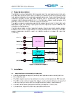
Ref
To FMC
TCXO
30.72MHz
Loop
Filter
REF_EN
To OUT
DAC 0
DAC 1
Clock
To GBT
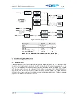
Figure 5: Clock tree
The AD9517 has four LVPECL outputs. OUT2 and OUT3 are used for clocking the DAC
devices. The other four clock outputs can be programmed either as LVDS or LVCMOS33.
These outputs have the ability to enable a programmable delay. OUT4 is connected to the
FMC connector for test and monitoring purposes. OUT5 connects to the gigabit transceiver
reference clock on the FMC connector (as a build option it can be connected to OUT7). OUT6
connects to the clock output on a MMCX connector.
4.9.1 PLL design
The PLL functionality of the AD9517 is used to operate from an internal sampling clock to
enable flexibility in frequency selection while maintaining high performance.
The default loop filter is designed for a phase detector frequency of 7.68MHz (f
ref
/4), loop
bandwidth of 10KHz, phase margin of 45 deg, and a charge pump of 4.8mA.
Lower phase detector frequencies might be required to achieve the required output clock
frequency (phase detector frequency equals the VCO tuning step size). Whether the loop filter
design still works for other configurations should be investigated case by case.