Panasonic PAN9420, Design Manual
The Panasonic PAN9420 is a cutting-edge device that combines convenience with outstanding performance. Make the most of its features by downloading the free Design Manual from manualshive.com, providing you with a comprehensive and user-friendly guide that ensures seamless integration and optimal utilization of this remarkable product.
Share
Download


Reviews:
No comments
Related manuals for PAN9420
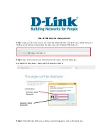
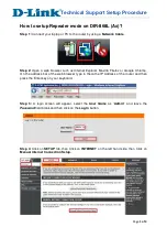
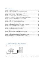
DSL-2750U
Brand: D-Link Pages: 3
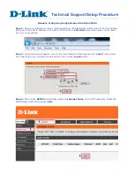
DSL-2750U
Brand: D-Link Pages: 3
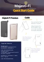
Premium
Brand: Majesti-Fi Pages: 2
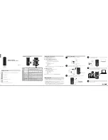
AC1200
Brand: D-Link Pages: 2
DIR-868L
Brand: D-Link Pages: 3

COVR-C1200
Brand: D-Link Pages: 24
DIR-868L
Brand: D-Link Pages: 59
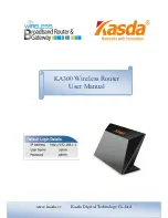
KA300
Brand: Kasda Pages: 42
MP980 series
Brand: Canon Pages: 4
DCS-5000L
Brand: D-Link Pages: 3
N300
Brand: D-Link Pages: 2
DAP-1720
Brand: D-Link Pages: 24
COVR-C1203
Brand: D-Link Pages: 6
DIR-850L
Brand: D-Link Pages: 13
COVR-2202
Brand: D-Link Pages: 2
SharePort DIR-825
Brand: D-Link Pages: 20
AirPlus DI-714P+
Brand: D-Link Pages: 5
AC5300
Brand: D-Link Pages: 12


