


xCORE-200 Clock Frequency Control
Register
Bitfield
Reset
Description
XS1_SSWITCH_PLL_CTL_NUM
[6:0]
Mode Pins R; PLL input divider stage =
R+1
XS1_SSWITCH_PLL_CTL_NUM
[20:8]
Mode Pins F; Multiplier stage of the PLL
= (F+1)/2
XS1_SSWITCH_PLL_CTL_NUM
[25:23] Mode Pins OD; PLL output divider stage
= OD+1
XS1_SSWITCH_PLL_CTL_NUM
30
N/A
LOCKN; ’0’ will force a wait
for PLL lock
XS1_SSWITCH_PLL_CTL_NUM
31
N/A
RESETN; ’0’ will force reset
on PLL change
XS1_SSWITCH_CLK_DIVIDER_NUM
[15:0]
0
System switch clock divider
= SSDIV+1. Reset value pro-
duces 400MHz for a 400MHz
system clock
XS1_SSWITCH_REF_CLK_DIVIDER_NUM
[15:0]
3
Reference clock divider = REF-
DIV+1. Reset value produces
100MHz for a 400MHz sys-
tem clock.
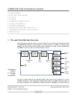
Figure 4:
Node Config-
uration
Registers
Register
Bitfield Reset Description
XS1_PSWITCH_PLL_CLK_DIVIDER_NUM
[15:0]
0
xCORE
Tile
clock
divider
=
XCDIV+1. Reset value produces
400MHz for an 400MHz system
clock
Figure 5:
Tile Configu-
ration control
registers
6.2
24MHz Oscillator
Use
MODE[1:0] = 11
, ie, leave any mode pins Not Connected. For the initial boot,
the system clock will be 100.0MHz, with the xCORE tile also running at 384 MHz.
The following are required:
R
= 0,
F
= 124,
OD
= 2. Write
0xC1007C00
to the PLL
Settings register in the Node Configuration to bring the PLL output up to 500MHz,
with code similar to the following:
# d e f i n e P L L _ 5 0 0 M H z 0 x 0 1 0 0 7 C 0 0
...
u n s i g n e d p l l C t r l R e a d D a t a ;
r e a d _ n o d e _ c o n f i g _ r e g ( t i l e [0] , X S 1 _ S S W I T C H _ P L L _ C T L _ N U M , p l l C t r l R e a d D a t a ) ;
if ( p l l C t r l R e a d D a t a != P L L _ 5 0 0 M H z ) {
w r i t e _ n o d e _ c o n f i g _ r e g ( t i l e [0] , X S 1 _ S S W I T C H _ P L L _ C T L _ N U M , P L L _ 5 0 0 M H z ) ;
}
...
XM010761A


