


xCORE-200 Clock Frequency Control
clock at 100MHz. In many applications this configuration will be selected, requiring
no reprogramming of the PLL or dividers. If the application requires a different
input frequency or system frequency then the PLL must be reprogrammed. The
xTIMEcomposer tools can be used to reprogram the PLL automatically by specifying
the application’s configuration in the XN file.
2
Constraints
There are a number of constraints on the frequencies of clocks at different points
on the xCORE-200 devices. These constraints must be met for the initial boot
sequence, and if the PLL is reprogrammed, for the reprogrammed values too.
Clock
Constraint
CLK
4.22–100.0 MHz
VCO frequency
260–1300 MHz
System clock
Maximum operating frequency—see device datasheet
Switch clock
System clock maximum
Reference clock
System clock maximum
xCORE Tile tiles clock System clock maximum
RGMII clock
System clock maximum
USB clock
12 or 24 MHz
Figure 2:
Clock
Frequency
Constraints
3
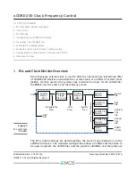
PLL Settings
There are three dividers within the PLL. R divides the input clock down. The next
divider divides the output of the voltage controlled oscillator (VCO) stage down to
the same frequency as the output of the R divider. Therefore this divider sets the
multiplication factor (F) of the PLL. The OD divider divides the output clock of the
VCO.
There is a constraint on the frequency of the clock at the comparator—the output
of R. There is another constraint placed on the output of the VCO.
4
Configuring the xCORE-200 Device
Some packages have mode pins that are used to determine the initial PLL settings
used after reset. This configuration must be such that all of the constraints are
met for the input clock driven onto CLK.
CLK Range (MHz) Mode 1 Mode 0 XCore Clock (MHz)
Multiplier OD
F
R
3.25-10 MHz
0
0
130-400 MHz
40
1
159
0
9-25 MHz
1
1
144-400 MHz
16
1
63
0
25-50 MHz
1
0
167-400 MHz
8
1
31
0
50-100 MHz
0
1
196-400 MHz
4
1
15
0
Figure 3:
Mode Pins
and Boot Con-
figuration
XM010761A


