FPGA Design Demonstration Board
Hardware User Guide
3-19
XC3020A FPGA and Socket (U4)
The XC3020A FPGA occupies socket U4 on the demonstration board.
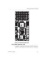
XC3020A Probe Points
All pins of the XC3020A FPGA connect to the headers that surround
the FPGA socket. These pins provide convenient points for probing
signals or making wirewrap connections to other circuitry, such as the
prototype area. Pin numbering increases from the inside row to the
outside, counterclockwise. See the corners of each header for the
starting number of that header. Refer to
for information.
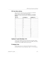
The XC3020A I/O pins 2 through 9 and 61 through 68 connect to
XC4003E pins 3 through 10 and 77 through 84, respectively. The
XC3020A pins share the XC4003E probe points header.
XC3020A Configuration Switches (SW1)
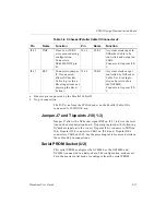
The following sections describe each of the SW1 switches. For more
information on configuring the XC3020A device, see the
INP-Input Switch (SW1-1)
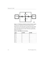
INP is an extra switch, which you can connect to provide an extra
logic input to the XC3020A pin 46 and the XC4003E pin 69. The FPGA
input pins are set to a logic "1" when the switch is on and a logic "0"
when the switch is off.
The FPGA pins connected to this switch are intended for use as
inputs. However, the pins have a 1 kilohm resistor that isolates them
from the switch. Therefore, the pins can be defined as outputs. It is
also possible to drive the pins from an external source by connecting
the source signal to the FPGA probe point header. See the following
figure for details.
Содержание MultiLINX DLC4
Страница 2: ...Hardware User Guide ...
Страница 10: ...Hardware User Guide vi Xilinx Development System ...
Страница 38: ...Hardware User Guide 1 24 Xilinx Development System ...
Страница 108: ...Hardware User Guide Glossary 4 Xilinx Development System ...

