


Available Motor Control Types
8-2 | CFW500
8
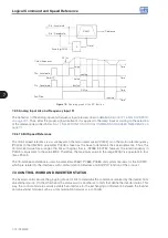
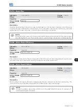
P0140 – Slip Compensation Filter
Adjustable
Range:
0 to 9999 ms
Factory
Setting:
500 ms
Properties:
V VW
Access Groups
via HMI:
Description:
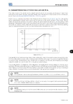
Time constant of the filter for slip compensation in the output frequency. You must consider a filter response
time equal to three times the time constant set in P0140 (500 ms).
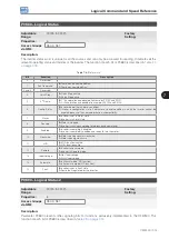
P0397 – Control Configuration
Adjustable
Range:
Bit 0 = Regen. Slip Comp.
Bit 1 = Dead Time Comp.
Bit 2 = Is Stabilization
Bit 3 = Red. P0297 in A0050
Factory
Setting:
000Bh
Properties:
cfg
Access Groups
via HMI:
Description:
This configuration parameter is input in hexadecimal form, with each bit having its meaning according to the
description below.
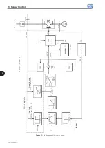
Slip Compensation during the Regeneration (Bit 0)
The regeneration is an operating mode of the inverter which occurs when the power flux goes from the motor
to the inverter. The Bit 0 of P0397 (set in 0) allows the slip compensation to be turned off in this situation. This
option is particularly useful when the compensation during the motor deceleration is necessary.
Dead Time Compensation (Bit 1)
The dead time is a time interval introduced in the PWM necessary for the commutation of the power inverter
bridge. On the other hand, the dead time generates distortions on the voltage applied to the motor, which can
cause torque reduction at low speeds and current oscillation in motors above 5 HP running with no load. Thus,
the dead time compensation measures the voltage pulse width in the output and compensates this distortion
introduced by the dead time.
Bit 1 of P0397 (set in 0) allows deactivating this compensation. This feature is useful when there is a problem
related to the inverter internal circuit for pulse feedback causing fault F0182. Thus, the compensation and the
fault can be disabled while the underlying cause of the problem cannot be solved.
Output Current Stabilization (Bit 2)
High-performance motors with power above 5 HP operate on the edge of stability, and may become unstable
when driven by frequency inverters and at operation with no load. Therefore, in this situation a resonance may
occur in the output current which may reach the overcurrent level F0070. Bit 2 of P0397 (set in 1) activates
a regulation algorithm of the output current in closed loop, which tries to compensate the resonant current
oscillations, improving the performance in low load / no load situations.
Reduction of P0297 in Alarm A0050 (Bit 3)
Bit 3 of P0397 controls the overtemperature protection action, refer to
Section 15.4 IGBTS OVERTEMPERATURE
Содержание CFW500 V1.8X
Страница 2: ......
Страница 4: ......
Страница 8: ...Contents...
Страница 34: ...General Information 2 4 CFW500...
Страница 38: ...About the CFW500 3 4 CFW500 3...
Страница 42: ...HMI and Basic Programming 4 4 CFW500 4...
Страница 52: ...Programming Basic Instructions 5 10 CFW500 5...
Страница 56: ...Identification of the Inverter Model and Accessories 6 4 CFW500 6...
Страница 76: ...Available Motor Control Types 8 4 CFW500 8...
Страница 84: ...V f Scalar Control 9 8 CFW500 9...
Страница 170: ...Communication 17 8 CFW500 17...