WM_PRJ_Q2400_PTS_005 -007
18th January 2006
Confidential©
All rights reserved
Page:
21
/
51
This document is the sole and exclusive property of WAVECOM. Not to be
distributed or divulged without prior written agreement.
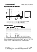
Typical implementation with SIM detection:
SIM_VCC 1
SIM_RST 2
SIM_DATA 7
SIM_PRES 8
VCC
RST
CLK
CC4
GND
VPP
I / O
CC8
GND
VCC 4
5
GND
100
k
Ω
C
100 nF
470pf
SIM_CLK 3
GND
GND
(1)
(2)
(1) Recommended components: DALC208SC6 (SGS-THOMSON).
(2) Recommended components: ESDA6V1SC6 (ST).
Figure 8 Example of 3V SIM Socket implementation
SIM socket connection:
SIM socket pin description
Signal Pin
number
Description
VCC 1
SIM_VCC
RST 2
SIM_RST
CLK 3
SIM_CLK
CC4 4
VCC
module
GND 5
GROUND
VPP 6
Not
connected
I/O 7
SIM_DATA
CC8 8
SIM_PRES with 100 k
Ω
pull down resistor
The capacitance value on the SIM_VCC must not exceed 100nF.
It is possible to use a capacitor value greater than 100nF but less than 330nF on
SIM_VCC, if an additional capacitor with a minimum value of 27µF (ESR <100
m
Ω
, X5R ceramic) is placed between VCC output (pin 40) and the GND.


