WM_PRJ_Q2400_PTS_005 -007
18th January 2006
Confidential©
All rights reserved
Page:
6
/
51
This document is the sole and exclusive property of WAVECOM. Not to be
distributed or divulged without prior written agreement.
List of Figures
Figure 1: Typical power supply voltage in GSM mode ...................................... 11
Figure 2: Maximal voltage ripple (Uripp) vs Frequency in GSM & DCS ............. 13
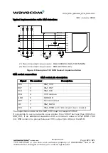
Figure 4: Example of SPI Bus typical implementation ....................................... 17
Figure 5: Example of keyboard implementation................................................. 18
Figure 6: Example of RS232 level shifter implementation.................................. 19
Figure 7: Example of Serial Link interface implementation ................................ 19
Figure 8 Example of 3V SIM Socket implementation ......................................... 21
Figure 9: Example of 1.8 V / 3 V SIM interface implementation......................... 22
Figure 10: Example of 3 V / 5 V SIM interface implementation.......................... 23
Figure 11: Example of ADC input implementation............................................. 24
Figure 12: Microphone decoupling capacitor .................................................... 25
Figure 13: Example of main microphone MIC2 implementation (differential
Figure 14: MIC1 inputs (differential connection) ............................................... 27
Figure 15: MIC1 inputs (single-ended connection)............................................ 28
Figure 16: Speaker outputs (differential mode).................................................. 29
Figure 17: Speaker outputs (single-ended connection)...................................... 29
Figure 18: Example of Buzzer implementation .................................................. 30
Figure 19: Example of battery implementation.................................................. 31
RST pin connection ........................................................................ 34
Figure 23: RTC supplied by a super capacitor ................................................... 36
Figure 24: RTC supplied by a battery cell with regulator................................... 37
Figure 25: RTC supplied by a non rechargeable battery .................................... 37
Figure 27: Antenna cable preparation (drawing not to scale) ............................ 40
Figure 28: Maximum bulk occupied on the application board ........................... 41
Figure 30: Example of serial link routing for downloading................................. 47
Figure 31: Download cable schematics (1/2)..................................................... 48
Figure 32: Download cable schematics (2/2)..................................................... 49


