P
P
r
r
a
a
c
c
t
t
i
i
c
c
e
e
T
T
E
E
L
L
E
E
C
C
O
O
M
M
S
S
O
O
L
L
U
U
T
T
I
I
O
O
N
N
S
S
F
F
O
O
R
R
T
T
H
H
E
E
2
2
1
1
S
S
T
T
C
C
E
E
N
N
T
T
U
U
R
R
Y
Y
TECHNICAL
TECHNICAL
Loop Detector Board with On Board
12 Volt Regulator
The
LDB-1
provides a loop activated contact
closure when used in series with telecom
devices on analog phone lines. The
LDB-1
will initiate a dry relay contact on any off-hook
condition. Alternatively, add the optional
PS-2
power supply to provide switched DC power.
The relay itself is phone line powered and
does not need an external power supply.
Because both TIP and RING currents flow
through the relay, excellent line balance is
maintained.
I
I
n
n
s
s
t
t
a
a
l
l
l
l
a
a
t
t
i
i
o
o
n
n
Dimensions:
47.6mm x 30.5mm (1.875” x 1.2”)
Mounting:
(2) #4 screws (not included) or foam tape (included)
Shipping Weight:
.45 kg (1 lb)
Added Loop Resistance:
40 ohms
Maximum Loop Current:
125 mA
Minimum Loop Current:
18 mA
Operating Temperature:
-26° to 54°C (-15° to 130° F)
Maximum Supply Voltage Input:
35 VDC
Maximum 12V Supply Current:
500 mA with PS-2
Longitudinal Balance:
63 dB minimum
Maximum Contact Voltage:
200 VDC
Maximum Contact Current:
500 mA
Maximum Contact Power:
10 W Resistive*
Connections:
7 pin screw terminal block
* Note:
If driving an inductive load a protection device must be
placed across terminals 6 and 7.
A
A
p
p
p
p
l
l
i
i
c
c
a
a
t
t
i
i
o
o
n
n
s
s
S
S
p
p
e
e
c
c
i
i
f
f
i
i
c
c
a
a
t
t
i
i
o
o
n
n
s
s
LDB-1
LDB-1
Loop Detect Board
March 9, 2012
• Provide relay closure on off-hook
• Trigger a security camera
• Trigger a tape recorder
• Phone “In Use” indicator
h
h
t
t
t
t
p
p
:
:
/
/
/
/
w
w
w
w
w
w
.
.
v
v
i
i
k
k
i
i
n
n
g
g
e
e
l
l
e
e
c
c
t
t
r
r
o
o
n
n
i
i
c
c
s
s
.
.
c
c
o
o
m
m
* Optional PS-2
Power Supply
(not included)
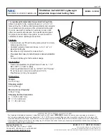
Installation Diagram
* Note:
If dry contacts are required, do NOT use the PS-2.
TIP
RING
Incoming
Phone Line
TIP
RING
Telcom
Device
N.O. Dry
Contacts
- or -
12V DC
Output
+
-
1
2
3
4
5
6
7
1
2
3
4
5
6
7
Schematic Diagram
+12V DC
COM
Due to the dynamic nature of the product design, the information contained in this document is subject to change without notice. Viking Electronics, and its affiliates and/or subsidiaries
assume no responsibility for errors and omissions contained in this information. Revisions of this document or new editions of it may be issued to incorporate such changes.
DOD# 406
ZF301230 Rev B
Printed in the U.S.A.
P
P
h
h
o
o
n
n
e
e
.
.
.
.
.
.
7
7
1
1
5
5
.
.
3
3
8
8
6
6
.
.
8
8
8
8
6
6
1
1


