


NINA-W1 series - System integration manual
UBX-17005730 - R15
Design-in
Page 32 of 54
C1 - Public
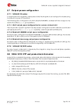
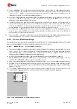
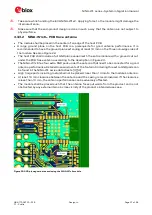
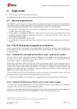
Figure 19: Transmission line trace design
To properly design a 50
Ω
transmission line, the following remarks should also be considered:
•
The designer should provide enough clearance from surrounding traces and ground in the same
layer; in general, a trace to ground clearance of at least two times the trace width should be
considered. The transmission line should also be ‘guarded’ by ground plane area on each side.
•
The characteristic impedance can be calculated as first iteration using tools provided by the layout
software. It is advisable to ask the PCB manufacturer to provide the final values that are usually
calculated using dedicated software and available stack-ups from production. It could also be
possible to request an impedance coupon on panel’s side to measure the real impedance of the
traces.
•
FR-4 dielectric material, although its high losses at high frequencies can be considered in RF
designs provided that:
o
RF trace length must be minimized to reduce dielectric losses.
o
If traces longer than few centimeters are needed, it is recommended to use a coaxial
connector and cable to reduce losses
o
Stack-up should allow for thick 50
Ω
traces and at least 200 µm trace width is
recommended to assure good impedance control over the PCB manufacturing process.
o
FR-4 material exhibits poor thickness stability and thus less control of impedance over
the trace length. Contact the PCB manufacturer for specific tolerance of controlled
impedance traces.
•
The transmission lines width and spacing to the GND must be uniform and routed as smoothly as
possible: route RF lines in 45 °C angle or in arcs.
•
Add GND stitching vias around transmission lines.
•
Ensure solid metal connection of the adjacent metal layer on the PCB stack-up to main ground
layer, providing enough vias on the adjacent metal layer.
•
Route RF transmission lines far from any noise source (as switching supplies and digital lines) and
from any sensitive circuit to avoid crosstalk between RF traces and Hi-impedance or analog
signals.
•
Avoid stubs on the transmission lines, any component on the transmission line should be placed
with the connected pad over the trace. Also avoid any unnecessary component on RF traces.


