TOBY-L4 series - System Integration Manual
UBX-16024839 - R04
Design-in
Page 102 of 143
2.8
Audio interface
2.8.1
Analog audio interface
2.8.1.1
Guidelines for analog audio uplink path circuit design
Guidelines for connecting two external microphones
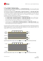
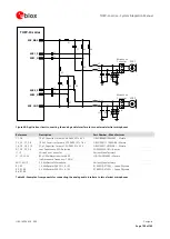
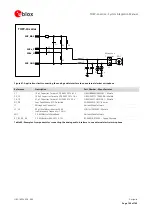
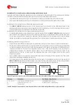
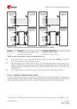
Figure 60 and Table 44 show an application circuit connecting the uplink path of the analog audio interface of
TOBY-L4 series modules to two electret microphones:
One external 2.2 k
electret microphone is connected to the
MIC1_P
/
MIC1_N
analog audio uplink path
One external 2.2 k
electret microphone is connected to the
MIC2_P
/
MIC2_N
analog audio uplink path
The first differential analog audio input (
MIC1_P
,
MIC1_N
) and the second differential analog audio input
(
MIC2_P
,
MIC2_N
) interfaces can be used alternatively, in mutually exclusive way. For example, one can be used
for voice call purposes, the other can be used for eCall purposes.
As in the example circuit in Figure 60 and Table 44, the following general guidelines are recommended for the
design of an analog audio circuit connecting two external electret microphones:
Provide a correct supply to the used electret microphones, as for example providing a clean connection from
the
MIC_BIAS
supply output to the microphones. It is suggested to implement a bridge structure:
o
The microphones, with their nominal intrinsic resistance value, represent one resistor of the bridge.
o
To achieve good supply noise rejection, the ratio of the two resistances in one leg (e.g. R2 / R3 resistors
in Figure 60) should be equal to the ratio of the two resistances in the other leg (e.g. R4 / MIC1),
meaning that R2 must be equal to R4 (e.g. 2.2 k
) and R3 must be equal to the microphone nominal
intrinsic resistance value (e.g. 2.2 k
for MIC1).
Using the
MIC_BIAS
supply output of the module, provide a suitable series resistor at the
MIC_BIAS
supply
output and then mount a suitable large bypass capacitor to provide additional supply noise filtering. See the
R1 and R5 series resistors (1.5 k
) and the C1 and C5 bypass capacitors (10 µF).
Do not place a bypass capacitor directly at the
MIC_BIAS
supply output, since a suitable internal bypass
capacitor is already provided to guarantee stable operation of the internal regulator.
Connect the reference of the microphone circuit to the
MIC_GND
pin of the module as a sense line.
Provide a suitable series capacitor at both
MIC1_P
/
MIC1_N
and
MIC2_P
/
MIC2_N
analog uplink inputs for
DC blocking (as the C2 / C3 and C7 / C8 100 nF Murata GRM155R71C104K capacitors in Figure 60). This
provides a high-pass filter for the microphone DC bias with the correct cut-off frequency according to the
value of the resistors of the microphone supply circuit. Then connect the signal lines to the microphone.
Provide the correct parts on each line connected to the external microphone as noise and EMI
improvements, to minimize RF coupling and TDMA noise, according to the custom application requirements.
o
Mount an 82 nH series inductor with a Self Resonance Frequency ~1 GHz (e.g. the Murata
LQG15HS82NJ02) on each microphone line (L1 / L2 and L3 / L4 inductors in Figure 60).
o
Mount a 27 pF bypass capacitor (e.g. Murata GRM1555C1H270J) from each microphone line to the
solid ground plane (C4 / C5 and C9 / C10 capacitors in Figure 60).
Use microphones designed for GSM applications, which typically have internal built-in bypass capacitor(s)
with Self-Resonant Frequency in the cellular frequency range(s).
Provide additional ESD protection (e.g. Bourns CG0402MLE-18G varistor) if the analog audio lines will be
externally accessible on the application device, according to the EMC/ESD requirements of the custom
application. Mount the protection close to an accessible point of the line (D1 / D2 and D3 / D4 in Figure 60).

