SARA-G3 series - System Integration Manual
UBX-13000995 - R06
Objective Specification
Design-in
Page 100 of 218
C5
C8
GND
C7
C6
C9
SARA-G3 series
52
VCC
53
VCC
51
VCC
+
USB
Supply
C3
R4
θ
U1
I
USB
I
AC
I
END
T
PRG
SD
V
IN
V
INSNS
MODE
ISEL
C2
C1
5V0
TH
GND
V
OUT
V
OSNS
V
REF
R1
R2
R3
Li-Ion/Li-Pol
Battery Pack
D1
B1
C4
Li-Ion/Li-Polymer
Battery Charger IC
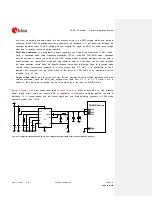
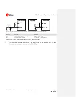
Figure 31: Li-Ion (or Li-Polymer) battery charging application circuit
Reference
Description
Part Number - Manufacturer
B1
Li-Ion (or Li-Polymer) battery pack with 470
NTC
Various manufacturer
C1, C4
1 µF Capacitor Ceramic X7R 0603 10% 16 V
GRM188R71C105KA12 - Murata
C2, C6
10 nF Capacitor Ceramic X7R 0402 10% 16 V
GRM155R71C103KA01 - Murata
C3
1 nF Capacitor Ceramic X7R 0402 10% 50 V
GRM155R71H102KA01 - Murata
C5
330 µF Capacitor Tantalum D_SIZE 6.3 V 45
m
T520D337M006ATE045 - KEMET
C7
100 nF Capacitor Ceramic X7R 0402 10% 16 V GRM155R61A104KA01 - Murata
C8
56 pF Capacitor Ceramic C0G 0402 5% 25 V
GRM1555C1E560JA01 - Murata
C9
15 pF Capacitor Ceramic C0G 0402 5% 25 V
GRM1555C1E150JA01 - Murata
D1
Low Capacitance ESD Protection
USB0002RP or USB0002DP - AVX
R1, R2
24 k
Resistor 0402 5% 0.1 W
RC0402JR-0724KL - Yageo Phycomp
R3
3.3 k
Resistor 0402 5% 0.1 W
RC0402JR-073K3L - Yageo Phycomp
R4
1.0 k
Resistor 0402 5% 0.1 W
RC0402JR-071K0L - Yageo Phycomp
U1
Single Cell Li-Ion (or Li-Polymer) Battery
Charger IC for USB port and AC Adapter
L6924U - STMicroelectronics
Table 17: Suggested components for Li-Ion (or Li-Polymer) battery charging application circuit
2.1.1.8
Guidelines for VCC supply layout design
Good connection of the module
VCC
pins with DC supply source is required for correct RF performance.
Guidelines are summarized in the following list:
All the available
VCC
pins must be connected to the DC source.
VCC
connection must be as wide as possible and as short as possible.
Any series component with Equivalent Series Resistance (ESR) greater than few milliohms must be
avoided.
VCC
connection must be routed through a PCB area separated from sensitive analog signals and
sensitive functional units: it is good practice to interpose at least one layer of PCB ground between
VCC
track and other signal routing.


