LILY-W1 series - System integration manual
UBX-15027600 - R09
Design-in
Page 27 of 64
C1 - Public
•
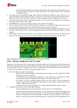
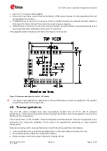
Pins from 1 to 25 should be NSMD.
•
Inner pins must have a good thermal bonding to PCB ground planes to help spreading the heat
generated by the module.
•
If NSMD design is chosen for inner pins, thermal reliefs should be considered and vias added on
those pins for heat sinking. Those vias may require copper capping.
•
If SMD design is chosen for inner pins, the land pattern can be flooded on a ground plane beneath
the module and vias added around the pins for heat sink.
The suggested paste mask layout follows the copper mask layout.
Figure 10: Recommended footprint for LILY-W1 module
⚠
The exact mask geometries, distances and stencil thicknesses must be adapted to the specific
production process of the customer.
2.8
Thermal guidelines
The LILY-W1 series modules have been successfully tested from -40 °C to +85 °C ambient
temperature. The board will generate heat during high loads that must be dissipated to sustain the
lifetime of the components.
The improvement of the module’s thermal dissipation will decrease its internal temperature, thus
increasing the long-term reliability of the device for applications operating at high ambient
temperature.
Recommended layout for best performance should follow the guidelines listed below:
•
Vias specification for ground filling: 300/600
μ
m, no thermal reliefs are allowed on vias
•
Ground vias density under the module: 50 vias/cm
2
•
Minimum layer count and copper thickness: 4 layers, 35
μ
m


