GPS
Modules
-
System
Integration
Manual
(SIM)
(incl.
Reference
Design)
Design-In
GPS.G4-MS4-05007-A1
Page 54
your position is our focus
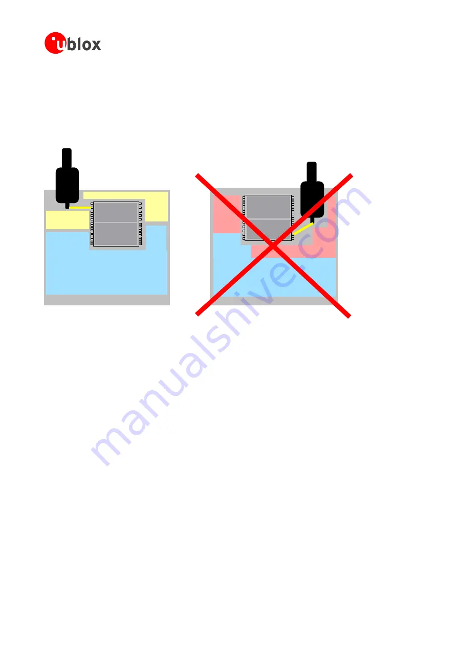
3.6.3 Placement
The
placement
of
the
ANTARIS
®
4
GPS
Receiver
on
the
PCB
is
very
important
to
achieve
maximum
GPS
performance.
The
connection
to
the
antenna
must
be
as
short
as
possible
to
avoid
jamming
into
the
very
sensitive
RF
section.
Make
sure
that
RF
critical
circuits
are
clearly
separated
from
any
other
digital
circuits
on
the
system
board.
To
achieve
this,
position
the
receiver
digital
part
towards
your
digital
section
of
the
system
PCB.
16
17
18
19
20
21
22
23
24
25
26
27
28
29
15
14
12
11
10
9
8
7
6
5
4
3
2
1
13
30
Non 'emitting'
circuits
PCB
Digital & Analog circuits
Non
'emitting'
circuits
An
te
n
n
a
Digital Part
RF Part
RF
'emitting'
circuits
PCB
Digital & Analog circuits
RF
'emitting'
circuits
An
tenna
16
17
18
19
20
21
22
23
24
25
26
27
28
29
15
14
12
11
10
9
8
7
6
5
4
3
2
1
13
30
Digital Part
RF Part
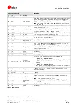
Figure 42: TIM placement
3.6.4 Antenna
Connection
and Grounding Plane Design
a
passive
patch
antenna
or
an
active
antenna.
The
antenna
RF
connection
is
on
the
PCB
and
connects
the
RF_IN
pin
with
the
antenna
feed
point
or
the
signal
pin
of
the
connector,
ANTARIS
®
4
can
be
either
connected
to
respectively.
Figure 43
illustrates
connection
to
a
typical
five-pin
RF
connector.
One
can
also
see
the
improved
shielding
for
digital
lines
according
to
the
discussion
in
Section
1.6.3
.
Depending
on
the
actual
size
of
the
ground
area,
additional
vias
should
be
placed
in
the
outer
region.
In
particular,
the
edges
of
the
ground
area
should
be
terminated
with
a
dense
line
of
vias.


