


Hangzhou Tuya Inc.
NM1 Module Hardware Design Manual
https://www.tuya.com
Page 21 of 29
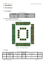
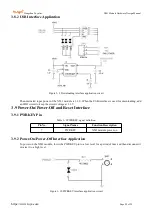
3.9.3 RESET Pin
Table 3- 10 RESET signal definition
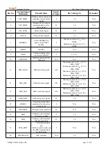
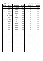
Pin No.
Signal Name
Function Description
15
RESET
NM1 module resetting
To reset the NM1 module, lower the RESET pin to a low level for a period of time and then disconnect it or
raise it to a high level.
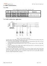
3.9.4 RESET Interface Application
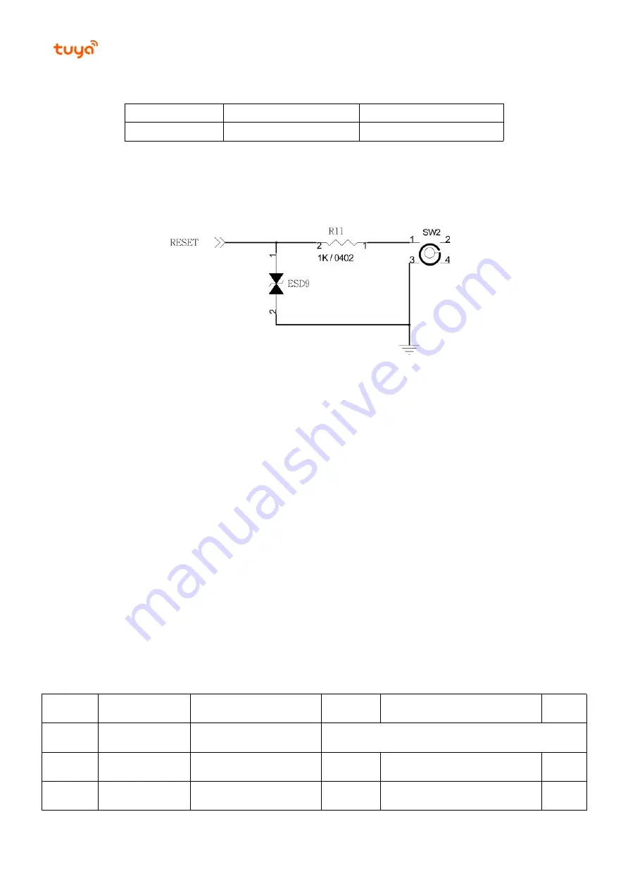
Figure 3- 11 RESET interface application circuit
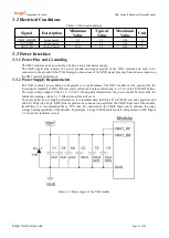
4 Design Instructions
This chapter provides general design guidance about the NM1 module to ensure a better product performance.
4.1 General Design Rules and Requirements
During peripheral circuit design, ensure that the external power supply have sufficient power and the differential
impedance of the USB 1.1 signal cable is within 90 ohms. Design general signal interfaces as required to match
the interface signal level and prevent the NM1 module being damaged due to inconsistent levels. The NM1
module has good RF indicator performance. You need to design the antenna circuit on the PCB as required and
control the impedance to prevent the RF indicators being affected.
4.2 Power Supply Circuit Design
The power supply on the PCB should supply 0.5 A or higher power to meet peak current requirements of the
NM1 module. The trace width on the PCB must be large enough and form good circulation with the ground. In
addition, add a large capacitor with over 1000 μF to the power supply circuit to ensure transient power supply,
and control the power ripple within 100 mV.
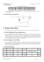
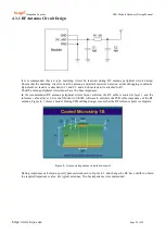
4.3 RF Circuit Design
34
GND
GND
N/A
N/A
N/A
35
RF_ANT
RF antenna
50 ohms characteristic impedance
36
GND
GND
N/A
N/A
N/A
37
GND
GND
N/A
N/A
N/A


