


User's Manual l TQMa8XxS UM 0101 l © 2022, TQ-Systems GmbH
Page 18
3.3
TQMa8XxS interfaces
To ensure flexible use of all i.MX 8X functions, all i.MX 8X pins or interfaces are routed to the module headers where possible and
are thus available on the base board. Besides some pins that are not available due to module-internal functions like LPDDR4 and
for technical reasons, there are minor restrictions in the availability of i.MX 8X pins, which are shown in the following table (only
functional pins mentioned):
Interface i.MX 8X
Quantity
Chapter
Note
EMMC0
1
Use for optional e-MMC, 8 bit
QSPI0A
1
Use for optional SPI-NOR flash
DDR
1
Use for LPDDR4, 32 bit
3.3.1
Gigbit Ethernet
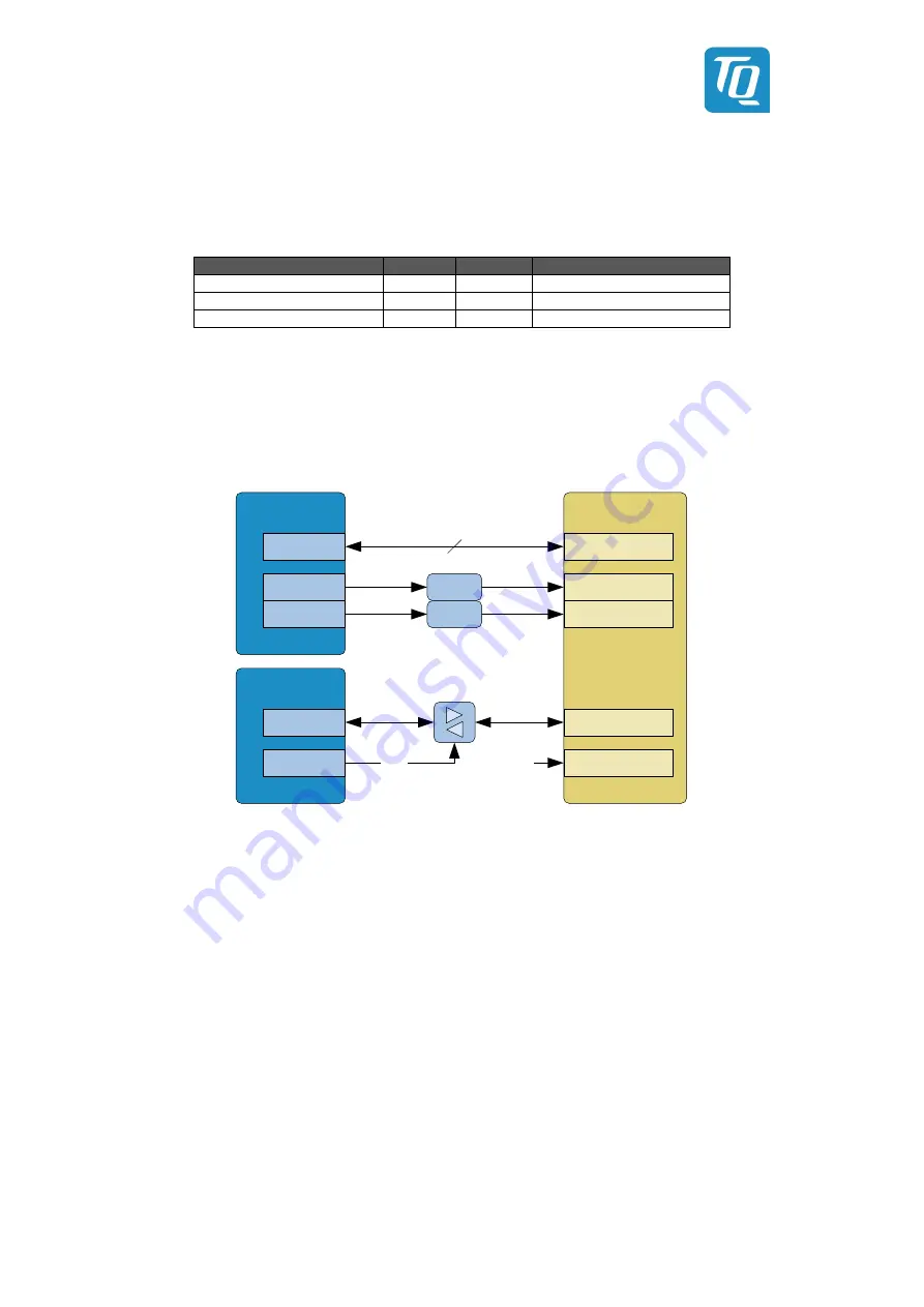
Two Gigabit Ethernet interfaces (GBE0, GBE1) are provided at the SMARC connector of the TQMa8XxS.
These are implemented with two independent PHYs. The LED signals are defined as 3.3 V tolerant open-drain outputs for a
current of at least 24 mA each.
i.MX 8X
DP83867
TD[A:D]
SMARC-Pins
GBEx_MDIx
GBEx_LINK1000#
GBEx_LINK_ACT#
GBE0_SDP
ENET0_REFC
LK_125M_25M
LED1
LED2
8
FET
FET
74LVC1T45
PCIE_CTRL0_
CLKREQ#
DIR
GBE1_SDP
NC
Figure 10:
Block diagram Ethernet
Only one of the IEEE 1588 signals GBE[1:0]_SDP is realized. Both ENET controllers of the i.MX 8X have one trigger signal (PPS)
each, but this signal is only multiplexable at the CPU ball F28. For the SDP signal, a bidirectional level converter from 1.8 V to 3.3
V is required. The SN74LVC1T45 from TI is used for this purpose. Since the data direction is application dependent, the signal of
the CPU ball PCIE_CTRL0_CLKREQ# configured as GPIO is used for direction control.
The GPIO pins of the PHY have internal pull-down resistors for strap configuration, which are switched off after power-up. Thus,
the data direction of the SDP signals is defined as input, but this affects the strap configuration. Since the input level of the SDP
signals is unknown, the corresponding strap configuration is undefined. For this reason it is mandatory that the corresponding
configuration registers are set by software. By default, the SDP signals are defined as input.
According to the SMARC standard, the Ethernet PHYs are part of the SMARC module, so that only the magnatics are
implemented on the carrier. Since the single-gigabit PHY DP83867ISRGZ has already proven itself several times, it is used on the
basis of the MBa8Xx. The connection to the CPU is done via RGMII.
Since the second PHY is optional, the provision of an IEEE 1588 trigger signal is only done at the SMARC GBE0_SDP pin, which is
connected to the CPU ball ENET0_REFCLK_125M_25M (see chapter 3.1.3.1).
The control of the activity LEDs is done by the LED-GPIOs of the respective PHYs.


