


1-4. Tray Replacement
Note:
• Perform this service only when a defective with a disc
not ejected, etc. occurs.
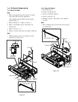
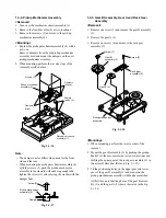
1-4-1. Tray Removal
1. Remove the mechanism chassis assembly. (Refer to
item 1-3-1.)
2. Turn the gear (2) clockwise to eject the tray (1).
3. Pull out the tray (1) to this side until it stops.
4. Release the claws on the right side of the mechanism
chassis assembly (part A) and pull out the tray (1) with
it obliquely lifted up.
Fig. 2-1-22
Tray (1)
Tray (1)
Gear (2)
Mechanism chassis
assembly
A
Claws
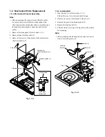
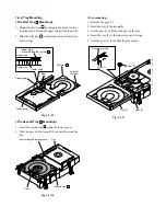
<The First Tray
1
Removal>
1. Slide the tray marked
1
in the arrow direction, then
remove it from two bosses.
Fig. 2-1-23
<The Second Tray
2
Removal>
1. Turning the gear counterclockwise ascends the tray.
Pull out the second tray marked
2
.
Fig. 2-1-24
First tray 1
Label of
first tray 1
Bosses
Upper Wing
Lower Wing
(for second tray)
Removed tray
1
Gear
Turn it
counterclockwise
Second tray 2
Содержание SD-2050
Страница 1: ...DVD VIDEO PLAYER SERVICE MANUAL May 2000 s FILE NO 810 200005 SD 2050 DIGITAL VIDEO ...
Страница 5: ...SECTION 1 GENERAL DESCRIPTIONS SECTION 1 GENERAL DESCRIPTIONS 1 OPERATING INSTRUCTIONS ...
Страница 51: ...47 Others Memo ...
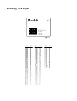
Страница 80: ...4 2 Power Supply Block Diagram Fig 3 4 2 ...
Страница 82: ...Fig 3 4 5 4 3 3 Front Display Power Switch Block Diagram ...
Страница 84: ...Fig 3 4 7 4 4 2 Logical System Block Diagram ...
Страница 85: ...4 5 Output Block Diagram Fig 3 4 8 ...
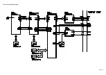
Страница 86: ...10 1 3 4 A B C D E G 2 5 6 7 8 9 F Fig 3 5 1 5 CIRCUIT DIAGRAMS 5 1 Power Supply Circuit Diagram ...
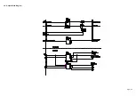
Страница 88: ...10 1 3 4 A B C D E G 2 5 6 7 8 9 F Fig 3 5 3 5 2 Front Display Power Switch Circuit Diagram ...
Страница 95: ...Fig 3 5 5 5 3 2 Main Circuit Diagram ...
Страница 96: ...5 3 2 Main Circuit Diagram ...
Страница 97: ......
Страница 98: ......
Страница 99: ......
Страница 100: ......
Страница 101: ......
Страница 102: ......
Страница 103: ...Fig 3 5 5 ...
Страница 105: ...Fig 3 5 6 10 1 3 4 A B C D E G 2 5 6 7 8 9 F 11 H 5 4 Output Circuit Diagram ...
Страница 115: ...10 1 3 4 A B C D E G 2 5 6 7 8 9 F Fig 3 6 6 EU01 Main PC Board Top pattern character symbol ...
Страница 116: ...10 1 3 4 A B C D E G 2 5 6 7 8 9 F Fig 3 6 7 EU01 Main PC Board Bottom pattern character symbol ...
Страница 120: ...4 EXPLODED VIEWS 4 1 Packing Assembly Fig 4 4 1 ZF01 ZF27 ZF17 ZF10 ZF11 ZF23 ZF30 ZK04 ZK01 ZK03 ZK02 ...
Страница 125: ......


