background image

www.ti.com

1

Description

2

Initial Configuration

2.1

Power Supply

3

Signals

3.1

Input Signals

3.2

Output Signals

3.3

TGC Outputs

Description

The Texas Instruments VCA8500BOARD evaluation module makes it easy to evaluate the performance of
the VCA8500 variable gain amplifier. The evaluation module operates in three modes: Default Power Up,
PC Control, and Direct Control. Default-Power-Up mode does not require any external clocking or data
input to enable the operation of the VCA8500. The functionality in Default-Power-Up mode is limited to
factory-programmed modes. PC-Control mode uses the included software to operate all of the functions of
the VCA8500. The software was written on Windows™ XP and its operation has been verified with
Windows™ XP. Direct-Control mode uses external control and data signals to control the functions of the
VCA8500.

The VCA8500BOARD has the following features:

Easy testing of the VCA8500

Single-ended input

Three modes of operation:

Default Power Up

PC Control

Direct Control

The VCA8500BOARD has provisions for six separate power supplies:

+5 V: Positive VCA Supply

This positive 5 V supplies the CW and VCA circuits. (P2)

+3.3 V: Positive VCA Supply

This positive 3.3 V supplies the LNA, Digital circuit and VCA Outputs . Ensure that all three pads of
W1 solder jumper are shorted. (P2)

+5 V/–5 V: Supplies for all other circuitry

These supplies all other +5 V/-5 V requirements onboard. (P4)

+15 V/–15 V: Supplies for CW Amplifiers

These supplies are optional for the CW amplifiers only. To drive these amplifiers with +15 V/–15 V,
W2 and W3 solder jumpers should be open. (P3)

The input signals are applied to SMA connectors J1 to J8. The input impedance of the VCA is 8 k

. The

inputs are ac-coupled into the LNA of the VCA8500 through 1-

µ

F capacitors and do not attenuate the

input signal.

The outputs of the evaluation module are located at SMA connectors J21 through J28 for the TGC
outputs, and J10 to J19 for the CW outputs. The outputs from the VCA8500 are buffered with operational
amplifiers.

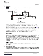
The differential TGC outputs are buffered by operational amplifiers (OPA842) in a differential configuration
with a differential gain of 1. When testing the VCA8500BOARD, outputs J21 through J28 (TGC outputs)
must be terminated into 50-

loads such as those of a spectrum analyzer. This termination results in the

proper matching for the output amplifiers, and no loss has to be taken into account.

2

VCA8500BOARD

SLOU216 – January 2008

Submit Documentation Feedback

Содержание VCA8500BOARD

Страница 1: ...ration 3 5 1 Default Power Up Mode 3 5 2 PC Control Mode 4 5 3 Direct Control Mode 4 6 VCA8500BOARD Full Access Software 4 6 1 Loading the Software 4 6 2 Initial Start up Screen 4 6 3 Other Program Fu...

Страница 2: ...W and VCA circuits P2 3 3 V Positive VCA Supply This positive 3 3 V supplies the LNA Digital circuit and VCA Outputs Ensure that all three pads of W1 solder jumper are shorted P2 5 V 5 V Supplies for...

Страница 3: ...ut capability To increase the output capability of the THS4021 ensure that W2 and W3 are open and supply 15 V to P3 The VCA8500BOARD contains a microcontroller to access internal functions The microco...

Страница 4: ...he entire device functionality is available for testing The software provides the ability to select any of the clamp ranges and PGA gains settings direct an input to any CW output or power down the co...

Страница 5: ...t program settings In order to activate these settings click Download When Reset is selected all options are set to these same default settings The Chip Power option only affects the VCA8500 and no ot...

Страница 6: ...channel Figure 4 shows this process Figure 4 CW Options Selection Once all the selections have been made click Download to send the data to the VCA8500 It is possible because of the flexible nature of...

Страница 7: ...xas Instruments Web site ti com by looking in the VCA8500 product folder in the Tools and Software section Selecting the Exit command button exits the program The Help pull down menu contains informat...

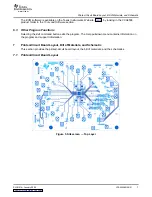
Страница 8: ...www ti com Printed Circuit Board Layout Bill of Materials and Schematic Figure 6 Ground Figure 7 Power Plane 1 8 VCA8500BOARD SLOU216 January 2008 Submit Documentation Feedback...

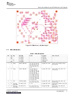
Страница 9: ...www ti com Printed Circuit Board Layout Bill of Materials and Schematic Figure 8 Power Plane 2 SLOU216 January 2008 VCA8500BOARD 9 Submit Documentation Feedback...

Страница 10: ...www ti com Printed Circuit Board Layout Bill of Materials and Schematic Figure 9 Ground 10 VCA8500BOARD SLOU216 January 2008 Submit Documentation Feedback...

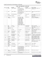
Страница 11: ...22 C24 Capacitor SMT 0402 Capacitor SMT 0402 CER 0 1 F C27 C34 C39 C42 10V 10 X5R C45 C48 C51 C52 C55 C56 C59 C62 C65 C68 C73 C76 C79 C82 C87 C89 C94 C95 C99 C101 C108 C110 C112 C117 C120 C124 C128 C1...

Страница 12: ...4 DUT SMT QFN RGC 64 0 5mm LS 9x9x1mm THRM PAD 15 4 Samtex TSW 106 05 G S P2 P4 P6 Header THU 6P Header 1X6 1CTR 16 1 Maxim MAX3221CAE U21 IC SMT 16P RS 232 Transceivers 17 10 TI THS4021CD U1 U10 IC S...

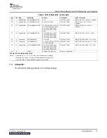
Страница 13: ...1k 1 1 16W R145 R149 R156 R158 R163 R165 R171 R183 R192 R197 R204 R206 32 9 Panasonic ERJ 2RKF4020X R173 R181 RES SMT 0402 RES SMT 0402 402 1 1 16W 33 10 Panasonic ERJ 2RKF6341X R1 R2 R11 R12 R37 R38...

Страница 14: ......

Страница 15: ......

Страница 16: ...oduct This notice contains important safety information about temperatures and voltages For additional information on TI s environmental and or safety programs please contact the TI application engine...

Страница 17: ...siness practice TI is not responsible or liable for any such statements TI products are not authorized for use in safety critical applications such as life support where a failure of the TI product wo...

Отзывы: