Texas Instruments UCC5870QDWJEVM-026 Скачать руководство пользователя страница 18

Low Voltage Test Procedure Example

www.ti.com

18

SLUUC64 – June 2020

Submit Documentation Feedback

Copyright © 2020, Texas Instruments Incorporated

UCC5870QDWJEVM-026 Evaluation Module User’s Guide

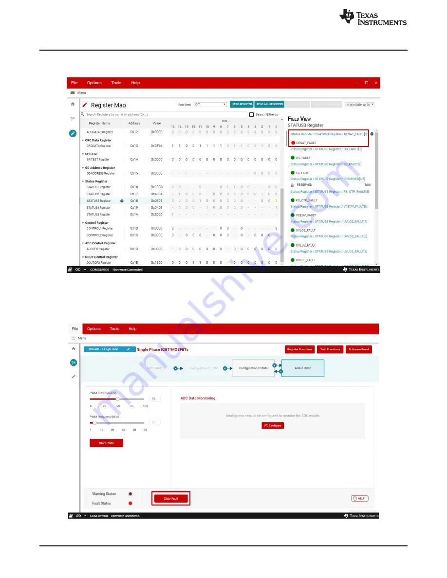
18. When there is a fault, read all status register and find out which fault was triggered in register map.
In the above example, it can be found that DESAT_FAULT is triggered.

Figure 21. Status Register Shows DESAT Fault

19. The fault can be reset by clicking "Clear fault" which writes 1 to CONTROL2 register bit[15]. Please

note ADC fault (Status 5 Register bit[15]) is on with default setting which selects external Vref for ADC
but the EVM board doesn't have external Vref, this fault can be cleared by selecting internal Vref.

Figure 22. Clear Fault Option

Содержание UCC5870QDWJEVM-026

Страница 1: ...is evaluation module has pin outputs that support the 820A 750V IGBT module FS820R08A6P2B connection for high power double pulses test and short circuit test Contents 1 General TI High Voltage Evaluation User Safety Guidelines 3 2 Description 5 3 Electrical Specifications 6 4 Test Summary 7 5 Low Voltage Test Procedure Example 10 6 High Voltage Test Example 23 7 Schematic 25 8 Layout Diagrams 27 9...

Страница 2: ...ress 0x01 21 29 Address SPI Mode High Side CF2 State 22 30 Address SPI Mode Low Side CF1 State Writing Address 0x02 22 31 EVM Primary and Secondary 23 32 EVM Connected with IGBT Module 24 33 Double Pulses Test Waveforms at 400V 100A 24 34 UCC5870 EVM Low Side Driver Schematic 25 35 UCC5870 EVM High Side Driver Schematic 26 36 PCB Layout Top Overlay 27 37 PCB Layout Top Layer 27 38 PCB Layout Inter...

Страница 3: ...ust be present in the area where the TI HV EVM and its interface electronics are energized indicating operation of accessible high voltages may be present for the purpose of protecting inadvertent access All interface circuits power supplies evaluation modules instruments meters scopes and other related apparatus used in a development environment exceeding 50 VRMS 75 VDC must be electrically locat...

Страница 4: ...e technical training and is designed to operate from an AC power supply or a high voltage DC supply Please read this user guide and the safety related documents that come with the EVM package before operating this EVM CAUTION Do not leave the EVM powered when unattended WARNING High Voltage Electric shock is possible when connecting board to live wire Board must be handled with care by a professio...

Страница 5: ...bus voltage sensing Primary and secondary ASC SPI based device reconfiguration verification supervision and diagnosis Compatible with 820A 750V IGBT module FS820R08A6P2B 2 2 I O Description Table 1 I O Description PINS DESCRIPTION TP 1 12V supply TP 2 Primary GND1 input TP 3 4 5V supply TP 4 Primary GND1 input TP 5 Test point for gate use for low voltage test only TP 6 Test point for source use fo...

Страница 6: ...per on J13 1 and J13 2 connect Vcc2 to the flyback supply output for the driver U4 Option A Option B Jumper not installed use external supply from TP7 for Vcc2 of the driver U4 J14 Option A Jumper on J14 1 and J14 2 connect Vee2 to the flyback supply output for the driver U4 Option A Option B Jumper not installed use external supply from TP7 for Vee2 of the driver U4 J15 Option A Jumper on J14 1 a...

Страница 7: ...setting 4 5 V there is LDO circuit on the board which will regulate voltage to 3 3V for the driver VCC1 Current limit 0 2 A DC power supply 2 Voltage setting 12 V as the input of the flyback power supply on the board Current limit 0 2 A 4 2 2 EVM GUI Program Installation UCC5870 Q1 EVM GUI program should be downloaded and installed This software requires GUI Composer runtime v7 4 1 You can downloa...

Страница 8: ...ure 2 left graph or right graph Figure 2 Jumper Settings for EVM MCU Daughter Board Address Mode SPI and Daisy Chain Mode SPI For the EVM board default jumper configuration as in Figure 3 should be adequate for this test Shunt 12 and shunt 16 are connecting the driver outputs with 100 nF load separately Shunt 10 and shunt 11 in the figure are setting up the driver with non differential input IN pi...

Страница 9: ...ch Setup For Low Voltage Test The current bench setup includes power supplies oscilloscope and GUI USB connections Follow the connection procedure below Figure 4 can be used as a reference Make sure the outputs of DC voltage power supplies are OFF before connection Connect 4 5V power supply to TP3 for primary VCC1 There are two options for the DC power supply connection for secondary power 1 Optio...

Страница 10: ...er Up CL 100 nF 1 Before proceeding to the power up procedure make sure that Section 4 2 4 is implemented for setting up all the equipment 2 Enable all power supplies 3 Open the GUI The home page should look like as Figure 6 The bottom pane should show Hardware Connected after few seconds In case it is not connected Click Options Serial port and choose the appropriate serial port from the list of ...

Страница 11: ...e 4 Click Explore the Device Modes page as Figure 7 should appear EVM number will be detected automatically select SPI type Regular SPI Address base SPI can be selected if MCU board is configured for this mode then click finish Figure 7 GUI EVM Number and SPI Mode Select 5 Select which driver high side or low side to program as in Figure 8 Figure 8 GUI High Side or Low Side Driver Selection ...

Страница 12: ...JEVM 026 Evaluation Module User s Guide 6 Then move to Configuration 1 State GUI will assign address for each driver during this state if address based SPI mode is selected for the previous step otherwise GUI has no action Figure 9 GUI Configuration 1 7 Move to Configuration 2 State in which the registers can be programmed Figure 10 GUI Configuration 2 ...

Страница 13: ... go to Register Map and click READ ALL REGISTERS Figure 11 GUI Configuration 2 Read All Registers 9 Then previously saved register file can be loaded by clicking File then load saved register or each register can be programmed separately with this GUI In this example let s disable DESAT protection first Otherwise Desat fault will trig as there is no IGBT connected Figure 12 GUI Configuration 2 Dis...

Страница 14: ... disable the gate voltage monitor function or change gate voltage monitor blanking time to 2500 ns and then change default state from HiZ to PL as this fault may be triggered with 100 nF load and 5 1 Ω gate resistor if tGMBLK 1000ns Figure 13 GUI Configuration 2 Disable Gate Voltage Monitor Function 11 Now move to Active State setup PWM duty cycle for 50 and PWM frequency for 10kHz Figure 14 GUI A...

Страница 15: ...20 Texas Instruments Incorporated UCC5870QDWJEVM 026 Evaluation Module User s Guide 12 After click Stark PWM PWM waveforms in Figure 15 will be generated Figure 15 Continuous PWM Waveforms 13 Stop PWM click Test Functions double pulse test parameters can be set up Figure 16 GUI Active State Double Pulses Test ...

Страница 16: ...as Instruments Incorporated UCC5870QDWJEVM 026 Evaluation Module User s Guide 14 Click Test double pulses waveforms in Figure 17 will be generated Figure 17 Double Pulses Test Waveforms 15 Next step go back to configuration 2 state and enable the DESAT protection Figure 18 GUI Configuration 2 Enable DESAT Protection ...

Страница 17: ...6 In active state generate a double pulse test faults status will become red since no IGBT is connected and connector for IGBT collector terminal is floating Figure 19 GUI Active Stage Fault Indicator 17 Figure 20 shows the waveforms of the Desat fault CH4 is the desat pin voltage when it reaches about 9 5V the fault is triggered and nFLT1 pin is pulled low Figure 20 DESAT Fault Test Waveforms ...

Страница 18: ...was triggered in register map In the above example it can be found that DESAT_FAULT is triggered Figure 21 Status Register Shows DESAT Fault 19 The fault can be reset by clicking Clear fault which writes 1 to CONTROL2 register bit 15 Please note ADC fault Status 5 Register bit 15 is on with default setting which selects external Vref for ADC but the EVM board doesn t have external Vref this fault ...

Страница 19: ...1 If using daisy chain mode SPI the MCU board jumpers need to be configured as in Figure 2 right graph then power up the supplies and the GUI should detect one EVM board select Daisy chain and click Finish Figure 23 Daisy Chain SPI Mode Selection 2 Then for HS GATE in Configuration 1 State click Proceed at this moment the driver will not move to configuration 2 stage Figure 24 Daisy Chain SPI Mode...

Страница 20: ...uide 3 Select LS GATE in Configuration 1 State click Proceed then both high side and low side driver will move to configuration 2 state at the same time Figure 25 Daisy Chain SPI Mode Low Side CF1 State 4 Below Figure 26 shows the GUI page of the above step when both high side and low side driver are in configuration 2 state Figure 26 Daisy Chain SPI Mode High Side and Low Side CF2 State ...

Страница 21: ...PI the MCU board jumpers need to be configured as in Figure 2 left graph then power up the supplies and the GUI should detect one EVM board select Address mode and click Finish Figure 27 Address SPI Mode Selection 2 Then for HS GATE in Configuration 1 State click Proceed GUI will write chip address 0x01 to the high side gate driver then it moves to configuration 2 state Figure 28 Address SPI Mode ...

Страница 22: ... 026 Evaluation Module User s Guide 3 Below Figure 29 shows the GUI page of the above step when high side driver is in configuration 2 state Figure 29 Address SPI Mode High Side CF2 State 4 Repeat the same step for the low side driver chip address 0x02 will be written to the low side driver Figure 30 Address SPI Mode Low Side CF1 State Writing Address 0x02 ...

Страница 23: ...ltage present when the EVM is connected to the IGBT module with high voltage DC bus The isolation components between primary and secondary are two flyback transformer and two UCC5870 gate drivers UCC5870 isolation capability is 3750 Vrms and flyback transformer ZA9710 AE not exactly the one shown in Figure 31 isolation capability is 3000 Vrms To minimize risk of electric shock hazard always follow...

Страница 24: ...shows how the EVM and MUC daughter card are connected with the IGBT module Additional DC bus capacitors and load inductor are needed for performance double pulses and short circuit test Please make sure all the connections are reliable and the test environment is safe before conducting any test Figure 32 EVM Connected with IGBT Module 6 3 Double Pulses Test Example Waveforms Figure 33 shows an exa...

Страница 25: ... Documentation Feedback Copyright 2020 Texas Instruments Incorporated UCC5870QDWJEVM 026 Evaluation Module User s Guide 7 Schematic Figure 34 and Figure 35 show the schematic diagram for the UCC5870 EVM Figure 34 UCC5870 EVM Low Side Driver Schematic ...

Страница 26: ...ic www ti com 26 SLUUC64 June 2020 Submit Documentation Feedback Copyright 2020 Texas Instruments Incorporated UCC5870QDWJEVM 026 Evaluation Module User s Guide Figure 35 UCC5870 EVM High Side Driver Schematic ...

Страница 27: ...tion Feedback Copyright 2020 Texas Instruments Incorporated UCC5870QDWJEVM 026 Evaluation Module User s Guide 8 Layout Diagrams Figure 36 to Figure 43 show the PCB layout information for the UCC5870 EVM Figure 36 PCB Layout Top Overlay Figure 37 PCB Layout Top Layer ...

Страница 28: ...i com 28 SLUUC64 June 2020 Submit Documentation Feedback Copyright 2020 Texas Instruments Incorporated UCC5870QDWJEVM 026 Evaluation Module User s Guide Figure 38 PCB Layout Inter Layer 1 Figure 39 PCB Layout Inter Layer 2 ...

Страница 29: ...grams 29 SLUUC64 June 2020 Submit Documentation Feedback Copyright 2020 Texas Instruments Incorporated UCC5870QDWJEVM 026 Evaluation Module User s Guide Figure 40 PCB Layout Inter Layer 3 Figure 41 PCB Layout Inter Layer 4 ...

Страница 30: ...i com 30 SLUUC64 June 2020 Submit Documentation Feedback Copyright 2020 Texas Instruments Incorporated UCC5870QDWJEVM 026 Evaluation Module User s Guide Figure 42 PCB Layout Bottom Layer Figure 43 PCB Layout Bottom Overlay ...

Страница 31: ...M 0 01 uF 100 V 10 X7R AEC Q200 Grade 1 0603 TDK CGA3E2X7R2A103K08 0AA C26 C66 2 CAP CERM 0 1 uF 50 V 10 X5R 0603 TDK C1608X5R1H104K080A A C27 C67 2 CAP CERM 0 1 uF 50 V 10 X7R AEC Q200 Grade 0 0805 Kemet C0805C104K5RACAUT O C37 1 CAP CERM 100 pF 50 V 5 C0G NP0 0402 Yageo America CC0402JRNPO9BN101 C38 C39 2 CAP CERM 22 uF 6 3 V 20 X5R 0603 MuRata GRM188R60J226MEA0 D D1 D14 2 Diode Zener 24 V 1 W P...

Страница 32: ...60330K0JNEA R12 R13 R15 R16 R47 R48 R49 R50 8 RES 100 5 0 1 W AEC Q200 Grade 0 0603 Vishay Dale CRCW0603100RJNEA R19 R33 R35 R36 R51 R66 R67 R68 R79 R80 10 RES 1 00 k 1 0 1 W AEC Q200 Grade 0 0603 Vishay Dale CRCW06031K00FKEA R20 R52 2 RES 33 5 0 1 W AEC Q200 Grade 0 0603 Vishay Dale CRCW060333R0JNEA R21 R30 R37 R38 R53 R62 R65 R69 R70 R78 R81 11 RES 0 5 0 1 W AEC Q200 Grade 0 0603 Vishay Dale CRC...

Страница 33: ...5 V Input 8 pin SON DRB 40 to 125 degC Green RoHS no Sb Br Texas Instruments TPS79601DRBR U4 U5 2 Isolated IGBT SiC MOSFET Gate Driver With Real Time Programmability DWJ0036A SOIC 36 Texas Instruments UCC5870 DWJ C36 C52 C53 C63 C76 C77 C78 C79 0 CAP CERM 100 pF 100 V 5 C0G NP0 AEC Q200 Grade 1 0603 MuRata GCM1885C2A101JA16 D FID1 FID2 FID3 0 Fiducial mark There is nothing to buy or mount N A N A ...

Страница 34: ...se resources are subject to change without notice TI grants you permission to use these resources only for development of an application that uses the TI products described in the resource Other reproduction and display of these resources is prohibited No license is granted to any other TI intellectual property right or to any third party intellectual property right TI disclaims responsibility for...

Отзывы: