DAC and ADC GUI Configuration File Changes When Using a Xilinx Development Platform
26
SLAU580B – June 2014 – Revised September 2016
Copyright © 2014–2016, Texas Instruments Incorporated
TSW14J10 FMC-USB Interposer Card
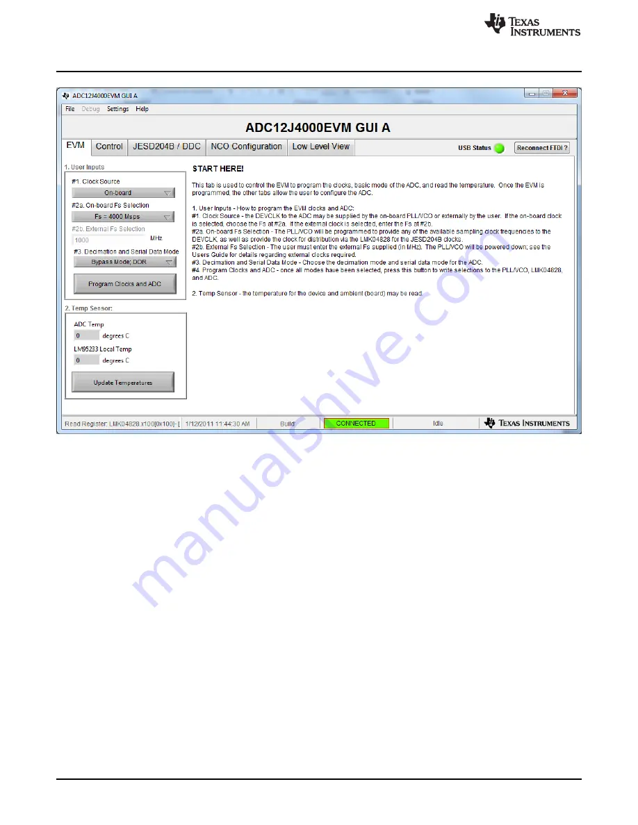
Figure 19. ADC12J4000EVM GUI
For this example, the lane rate is 8 Gbps. Using the equation in
for lane rates greater than 3.2
Gbps:
Reference clock
= Lane Rate / 20
8G / 20
= 400 MHz
Core clock
= Lane Rate / 40
8G / 40
= 200 MHz
Since the LMK04828 input clock (2 GHz) is the ADC sample clock divided by 2, to achieve the proper
frequency for the reference clock, this must be divided by 5. To achieve the proper core clock frequency,
this must be divided by 10.
After the ADC12J4000 EVM has been configured, in the GUI, click on the
Low Level View
tab and perform
the following writes to provide the proper divider for the LMK04828 outputs used by the Xilinx FPGA:
1. Go to LMK04828 address 0x110 and enter a “5” in the write data box and click the
Write Register
button.
2. Click the
Read Register
button and verify a “5” is read back.
3. Go to address 0x100, do a
Read Register
and verify the value “A” is read back. If not, write this value
to this address.


