SLOU186F
–
AUGUST 2006
–
REVISED AUGUST 2010
4.4
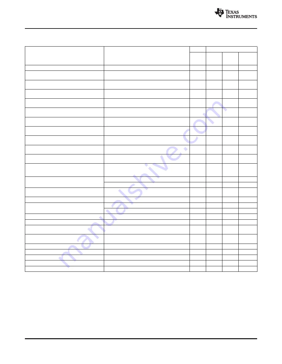
ELECTRICAL CHARACTERISTICS
over temperature range V
S
= 5 V (unless otherwise noted)
TYP
–
40
°
C
PARAMETER
CONDITIONS
MIN/
25
°
C
TO
UNIT
MAX
110
°
C
I
PD
Supply current in power-down mode
All systems disabled, including supply-voltage regulators
1
10
μ
A
MAX
The reference voltage generator and the VDD_X remain
I
PD2
Supply current in power-down mode 2
120
300
μ
A
MAX
active to support external circuitry.
Oscillator running, supply-voltage regulators in
I
STBY
Supply current in standby mode
1.5
4
mA
MAX
low-consumption mode
Supply current without antenna driver
Oscillator, regulators, Rx and AGC, are all active. Tx is
I
ON1
10
16
mA
MAX
current
off.
Supply current with antenna driver
Oscillator, regulators, Rx, AGC, and Tx are all active.
I
ON2
70
mA
MAX
current
Pout = 100 mW.
Supply current with antenna driver
Oscillator, regulators, Rx, AGC, and Tx are all active.
I
ON3
120
mA
MAX
current
Pout = 200 mW.
1.4
MIN
BG
Band Gap voltage
Internal analog reference voltage
1.6
V
1.7
MAX
1.4
MIN
V
POR
Power on reset voltage (POR)
2
V
2.5
MAX
3.1
MIN
V
DD_A
Regulated supply for analog circuitry
3.5
V
3.8
MAX
4
MIN
V
DD_RF
Regulated supply for RF circuitry
Regulator set for 5-V system with 250-mV difference.
4.6
V
5.2
MAX
3.1
MIN
V
DD_X
Regulated supply for external circuitry
3.4
V
3.8
MAX
The difference between the external supply and the
Rejection of external supply noise on
P
PSRR
regulated voltage is higher than 250 mV. Measured at
26
20
dB
MIN
the supply VDD_RF regulator
212 kHz.
Half-power mode
8
12
Ω
MAX
R
RFOUT
PA driver output resistance
Full- power mode
4
6
Ω
MAX
5
MIN
R
RFIN
RX_IN1 and RX_IN2 input resistance
10
k
Ω
20
MAX
V
RFIN
Maximum input voltage
At RX_IN1 and RX_IN2 inputs
3.5
V
PP
MAX
f
SUB-CARRIER
= 424 kHz
1.2
2.5
mV
PP
MAX
V
SENS
Input sensitivity
f
SUB-CARRIER
= 848 kHz
1.2
3
mV
PP
MAX
t
SET_PD
Set up time after power down
10
20
ms
MAX
t
SET_STBY
Set up time after standby mode
30
100
μ
s
MAX
Recovery time after modulation
t
REC
Modulation signal: sine, 424-kHz, 10-mVpp
60
μ
s
MAX
(ISO14443)
30
MIN
f
SYS_CLK
SYS_CLK frequency
In PD2 mode EN = 0 and EN2 = 1
60
kHz
120
MAX
CLK
MAX
Maximum CLK frequency
2
MHz
TYP
V
IL
Input logic low
0.2
0.2
VDD_I/O
MAX
V
IH
Input logic high
0.8
VDD_I/O
MIN
R
OUT
Output resistance I/O_0 to I/O_7
low_io = H for VDD_I/O
<
2.7 V
400
800
Ω
MAX
R
SYS_CLK
Output resistance SYS_CLK
low_io = H for VDD_I/O
<
2.7 V
200
400
Ω
MAX
8
ELECTRICAL SPECIFICATIONS
Copyright
©
2006
–
2010, Texas Instruments Incorporated
focus.ti.com:


