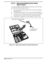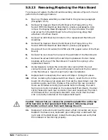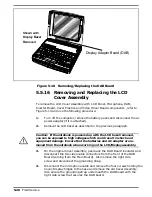
5.5.6
Opening/Replacing the Base Cover
Assembly
The Top Cover Assembly protects all internal components housed in the
base assembly (Boards, Floppy Drive, Speaker, etc. To open up the Base
Assembly for maintenance operations, perform the following procedure:
n
Note:
Removing the Top Cover Assembly will cause the PCMCIA Button
(P/N 9786086-1) and the Tamper Evident Warranty Label (P/N 9798834-2)
to become unusable. Ensure that these components are in stock before re-
moving the Top Cover.
1.
Power down the notebook, remove the battery packs, and disconnect the
AC Adapter, if installed.
2.
Disconnect any peripheral device interface cables from the external
interface connectors and remove any installed PCMCIA options.
3.
Remove the Keyboard Assembly as described in Paragraph 5.5.3.
4.
Open the notebook. Using a small straight slot screwdriver, gently pry
at the base of the two hinge covers (one on each side of the notebook)
and remove both hinge covers; set these aside for later installation.
5.
Close the notebook and then rotate the notebook such that the rear
connectors are facing the front. Remove the two Torx head screws,
one adjacent to each notebook hinge. Tape this set of screws together.
4.
With the notebook open, remove the three Torx-head screws and two
Phillips head screws from the perimeter of the keyboard recessed
area. Using tape, tape the screws together for ease of installation
later (label if you have difficulty remembering which screws go where).
5.
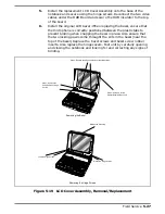
Close the Display Cover and flip the notebook over. Remove the three
Torx head screws from the three recessed areas (Figure 5-9) using the
long shank Torx driver. Then remove the Torx head screw located
under the Taper Evident Label near the Hard Drive assembly. Tape
this set of screws together.
6.
Place a 1" thick, 8-1/2" X 11" book on the work surface behind the
notebook. Flip the notebook right side up with the floppy drive facing
outwards. Then lift upwards gently allowing the Display and the Top
Cover Assembly to lay back over the book as a support.
7.
Replacement is essentially the reverse of Steps 1 through 6 above.
n
Note:
Do not replace the PCMCIA buttons and Warranty Label until
After
the unit has passed all tests.
5-14
Field Service
Содержание TravelMate 5000 Series
Страница 1: ...Maintenance Manual TravelMate 5000 Series Notebook Computers 9786166 0001 March 1995 ...
Страница 47: ...Figure 1 16 TM5000 Series Functional Block Diagram 1 30 General Description ...
Страница 95: ...Figure 4 2 Notebook Detailed Block Diagram Troubleshooting Procedures 4 3 ...
Страница 149: ...Figure 6 4 Main Board P54 75MHz P N 9798803 0001 Sheet 2 of 2 6 14 Illustrated Parts Listing ...
Страница 161: ...Figure 6 5 Figure 6 5 PCMCIA Sound Board P N 9786205 0001 Sheet 1 of 2 6 26 Illustrated Parts Listing ...
Страница 162: ...Figure 6 6 Figure 6 5 PCMCIA Sound Board P N 9786205 0001 Sheet 2 of 2 Illustrated Parts Listing 6 27 ...
Страница 172: ...Figure 6 7 Keyscan Board P N 9786209 0001 Illustrated Parts Listing 6 37 ...
Страница 180: ...Figure 6 11 Inverter Board P N 9786134 0001 Illustrated Parts Listing 6 45 ...
Страница 185: ...Figure 6 12 DAB Board P N 9786273 0001 6 50 Illustrated Parts Listing ...
Страница 188: ...Figure 7 1 Figure 7 1 Main Board Part No 9798803 Logic Diagram Sheet 1 of 22 7 2 Schematic Diagrams ...
Страница 189: ...Figure 7 1 Figure 7 1 Main Board Part No 9798803 Logic Diagram Sheet 2 of 22 Schematic Diagrams 7 3 ...
Страница 190: ...Figure 7 1 Figure 7 1 Main Board Part No 9798803 Logic Diagram Sheet 3 of 22 7 4 Schematic Diagrams ...
Страница 191: ...Figure 7 1 Figure 7 1 Main Board Part No 9798803 Logic Diagram Sheet 4 of 22 Schematic Diagrams 7 5 ...
Страница 192: ...Figure 7 1 Figure 7 1 Main Board Part No 9798803 Logic Diagram Sheet 5 of 22 7 6 Schematic Diagrams ...
Страница 193: ...Figure 7 1 Figure 7 1 Main Board Part No 9798803 Logic Diagram Sheet 6 of 22 Schematic Diagrams 7 7 ...
Страница 194: ...Figure 7 1 Figure 7 1 Main Board Part No 9798803 Logic Diagram Sheet 7 of 22 7 8 Schematic Diagrams ...
Страница 195: ...Figure 7 1 Figure 7 1 Main Board Part No 9798803 Logic Diagram Sheet 8 of 22 Schematic Diagrams 7 9 ...
Страница 196: ...Figure 7 1 Figure 7 1 Main Board Part No 9798803 Logic Diagram Sheet 9 of 22 7 10 Schematic Diagrams ...
Страница 197: ...Figure 7 1 Figure 7 1 Main Board Part No 9798803 Logic Diagram Sheet 10 of 22 Schematic Diagrams 7 11 ...
Страница 198: ...Figure 7 1 Figure 7 1 Main Board Part No 9798803 Logic Diagram Sheet 11 of 22 7 12 Schematic Diagrams ...
Страница 199: ...Figure 7 1 Figure 7 1 Main Board Part No 9798803 Logic Diagram Sheet 12 of 22 Schematic Diagrams 7 13 ...
Страница 200: ...Figure 7 1 Figure 7 1 Main Board Part No 9798803 Logic Diagram Sheet 13 of 22 7 14 Schematic Diagrams ...
Страница 201: ...Figure 7 1 Figure 7 1 Main Board Part No 9798803 Logic Diagram Sheet 14 of 22 Schematic Diagrams 7 15 ...
Страница 202: ...Figure 7 1 Figure 7 1 Main Board Part No 9798803 Logic Diagram Sheet 15 of 22 7 16 Schematic Diagrams ...
Страница 203: ...Figure 7 1 Figure 7 1 Main Board Part No 9798803 Logic Diagram Sheet 16 of 22 Schematic Diagrams 7 17 ...
Страница 204: ...Figure 7 1 Figure 7 1 Main Board Part No 9798803 Logic Diagram Sheet 17 of 22 7 18 Schematic Diagrams ...
Страница 205: ...Figure 7 1 Figure 7 1 Main Board Part No 9798803 Logic Diagram Sheet 18 of 22 Schematic Diagrams 7 19 ...
Страница 206: ...Figure 7 1 Figure 7 1 Main Board Part No 9798803 Logic Diagram Sheet 19 of 22 7 20 Schematic Diagrams ...
Страница 207: ...Figure 7 1 Figure 7 1 Main Board Part No 9798803 Logic Diagram Sheet 20 of 22 Schematic Diagrams 7 21 ...
Страница 208: ...Figure 7 1 Figure 7 1 Main Board Part No 9798803 Logic Diagram Sheet 21 of 22 7 22 Schematic Diagrams ...
Страница 209: ...To Be Supplied Figure 7 1 Figure 7 1 Main Board Part No 9798803 Logic Diagram Sheet 22 of 22 Schematic Diagrams 7 23 ...
Страница 210: ...Figure 7 2 Figure 7 2 PCMCIA Sound Board P N 9786205 Logic Diagram Sheet 1 of 12 7 24 Schematic Diagrams ...
Страница 211: ...Figure 7 2 Figure 7 2 PCMCIA Sound Board P N 9786205 Logic Diagram Sheet 2 of 12 Schematic Diagrams 7 25 ...
Страница 212: ...Figure 7 2 Figure 7 2 PCMCIA Sound Board P N 9786205 Logic Diagram Sheet 3 of 12 7 26 Schematic Diagrams ...
Страница 213: ...Figure 7 2 Figure 7 2 PCMCIA Sound Board P N 9786205 Logic Diagram Sheet 4 of 12 Schematic Diagrams 7 27 ...
Страница 214: ...Figure 7 2 Figure 7 2 PCMCIA Sound Board P N 9786205 Logic Diagram Sheet 5 of 12 7 28 Schematic Diagrams ...
Страница 215: ...Figure 7 2 Figure 7 2 PCMCIA Sound Board P N 9786205 Logic Diagram Sheet 6 of 12 Schematic Diagrams 7 29 ...
Страница 216: ...Figure 7 2 Figure 7 2 PCMCIA Sound Board P N 9786205 Logic Diagram Sheet 7 of 12 7 30 Schematic Diagrams ...
Страница 217: ...Figure 7 2 Figure 7 2 PCMCIA Sound Board P N 9786205 Logic Diagram Sheet 8 of 12 Schematic Diagrams 7 31 ...
Страница 218: ...Figure 7 2 Figure 7 2 PCMCIA Sound Board P N 9786205 Logic Diagram Sheet 9 of 12 7 32 Schematic Diagrams ...
Страница 219: ...Figure 7 2 Figure 7 2 PCMCIA Sound Board P N 9786205 Logic Diagram Sheet 10 of 12 Schematic Diagrams 7 33 ...
Страница 220: ...Figure 7 2 Figure 7 2 PCMCIA Sound Board P N 9786205 Logic Diagram Sheet 11 of 12 7 34 Schematic Diagrams ...
Страница 221: ...Figure 7 2 Figure 7 2 PCMCIA Sound Board P N 9786205 Logic Diagram Sheet 12 of 12 Schematic Diagrams 7 35 ...
Страница 222: ...Figure 7 3 Figure 7 3 Keyscan Board P N 9786209 Logic Diagram Sheet 1 of 5 7 36 Schematic Diagrams ...
Страница 223: ...Figure 7 3 Figure 7 3 Keyscan Board P N 9786209 Logic Diagram Sheet 2 of 5 Schematic Diagrams 7 37 ...
Страница 224: ...Figure 7 3 Figure 7 3 Keyscan Board P N 9786209 Logic Diagram Sheet 3 of 5 7 38 Schematic Diagrams ...
Страница 225: ...Figure 7 3 Figure 7 3 Keyscan Board P N 9786209 Logic Diagram Sheet 4 of 5 Schematic Diagrams 7 39 ...
Страница 226: ...Figure 7 3 Figure 7 3 Keyscan Board P N 9786209 Logic Diagram Sheet 5 of 5 7 40 Schematic Diagrams ...
Страница 227: ...Figure 7 4 Figure 7 4 Sleep Switch Board P N 9786148 Logic Diagram Sheet 1 of 1 Schematic Diagrams 7 41 ...
Страница 228: ...Figure 7 5 Figure 7 5 IR Board P N 9798813 Logic Diagram Sheet 1 of 2 7 42 Schematic Diagrams ...
Страница 229: ...Figure 7 5 Figure 7 5 IR Board P N 9798813 Logic Diagram Sheet 2 of 2 Schematic Diagrams 7 43 ...
Страница 230: ...Figure 7 6 Figure 7 6 LED Board P N 9796128 Logic Diagram Sheet 1 of 2 7 44 Schematic Diagrams ...
Страница 231: ...Figure 7 6 Figure 7 6 LED Board P N 9796128 Logic Diagram Sheet 2 of 2 Schematic Diagrams 7 45 ...
Страница 232: ...Figure 7 7 Figure 7 7 8 16 MB RAM Exp Board P N 9798816 Logic Diagram Sheet 1 of 1 7 46 Schematic Diagrams ...
Страница 233: ...Figure 7 8 Figure 7 8 Inverter Board P N 9796134 Logic Diagram Sheet 1 of 2 Schematic Diagrams 7 47 ...
Страница 234: ...Figure 7 8 Figure 7 8 Inverter Board P N 9796134 Logic Diagram Sheet 2 of 2 7 48 Schematic Diagrams ...
Страница 235: ...Figure 7 8 Figure 7 9 Display Adapter Board P N 9786273 Logic Diagram Sheet 1 of 3 Schematic Diagrams 7 49 ...
Страница 236: ...Figure 7 9 Figure 7 9 Display Adapter Board P N 9786273 Logic Diagram Sheet 2 of 3 7 50 Schematic Diagrams ...
Страница 237: ...Figure 7 9 Figure 7 9 Display Adapter Board P N 9786273 Logic Diagram Sheet 3 of 3 Schematic Diagrams 7 51 ...
Страница 239: ...Figure A 1 Code Page 437 United States A 2 Character Sets ...
Страница 240: ...Figure A 2 Code Page 850 Multilingual Character Sets A 3 ...
Страница 241: ...Figure A 3 Code Page 863 Canadian French A 4 Character Sets ...
Страница 242: ...Figure A 4 Code Page 865 Nordic Character Sets A 5 ...
Страница 286: ...Printed in U S A ...


