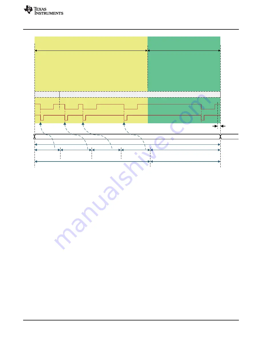
WD Response WINDOW 1
Programmed through the WDT_WIN1_CFG register
(0.55 ms to 140.8 ms in 0.55-ms steps)
WD Response WINDOW 2
Programmed through the WDT_WIN2_CFG register
(0.55 ms to 17.6 ms in 0.55-ms steps)
Three correct SPI WD question responses must be scheduled in this interval, in the correct
order:
After the t
WD_RESP_WIN1
time elapses, the WD response WINDOW 2 begins.
Responses (
answers
) are written to the WDT_ANSWER register.
The SPI WD question- response sequence order is important.
The final correct SPI-WD question response
(WD_ANSWER_RESP_0) must be scheduled in this time
interval.
After the last correct SPI-WD answer response, the next
WD question is generated within 1 system clock cycle
(typically 125 ns), after which the next WD response
WINDOW 1 (Q&A+1) starts
WD_ANSWER_
RESP_3
WD_ANSWER_
RESP_2
WD_ANSWER_
RESP_1
WD_ANSWER_
RESP_0
SPI WD Question Sequence Responses
(2)
WD Question Response Sequence
WD Question
Request
RD_WD_
QUESTION
SPI Question
Required
(1)
SPI
Commands
NCS pin
1 internal system clock cycle (125 ns)
to generate a new WD question for Q&A+1
Q&A [n]
Q&A [n + 1]
t
WD_RESP_WIN1
+ t
WD_RESP_WIN2
x
WD_ANSWER_RESP_3
x
WD_ANSWER_RESP_2
x
WD_ANSWER_RESP_1
Answer0 to
Question
Question to
Answer3
Answer3 to
Answer2
Answer2 to
Answer1
Answer1 to
Answer0
WINDOW 1 Duration
WINDOW 2 Duration
TPS65313 GUI
9
SLDU028A – January 2018 – Revised March 2020
Copyright © 2018–2020, Texas Instruments Incorporated
TPS65313-EVM User’s Guide
Figure 5. Watchdog Window Timing Diagram
describes the watchdog implementation on the MSP430™ MCU on the EVM.
6.1.7
MCU Error Signal Monitor (ESM)
The MCU error monitoring function is implemented in the GUI to check the functionality of MCU_ERR pin.
Both PWM mode and TMS570 mode of error monitoring is implemented on the GUI. Each setting is
described as follows:
TMS570 Mode button —
This option reads the register values and populates the corresponding text field
with the corresponding low and high periods.
Write MCU Error Window Registers button —
When enabled, the timing thresholds set in the text field
are written to the corresponding device timing registers (PWM_LMAX, PWM_LMIN, PWM_HMAX,
PWM_HMIN).
Enable PWM Output button —
The
Low Duration
,
High Duration
, and the
Enable PWM Output
options
turn on the clock with those periods on the MCU GPIO connected to the MCU_ERR pin. Jumper
J11 must be set between pin 2 and pin 3 for this signal to be applied to the device pin.
MCU Error Window Register Values fields —
This option reads the timing register values and
populates the corresponding text field with the corresponding low and high periods.
The ESM is disabled by default, and can be activated by setting the MCU_ESM_EN bit to 1b in the
SAFETY_CHECK_CTRL SPI register.
6.1.8
SPI Status Bits
The SPI status flag response byte of the device is displayed in this section of the
Device Controls
page.
For more information, refer to the
TPS65313-Q1 Wide-VIN Power-Management IC for Automotive
Applications
datasheet.


