background image

6 Board Setup

6.1 Supply Voltage

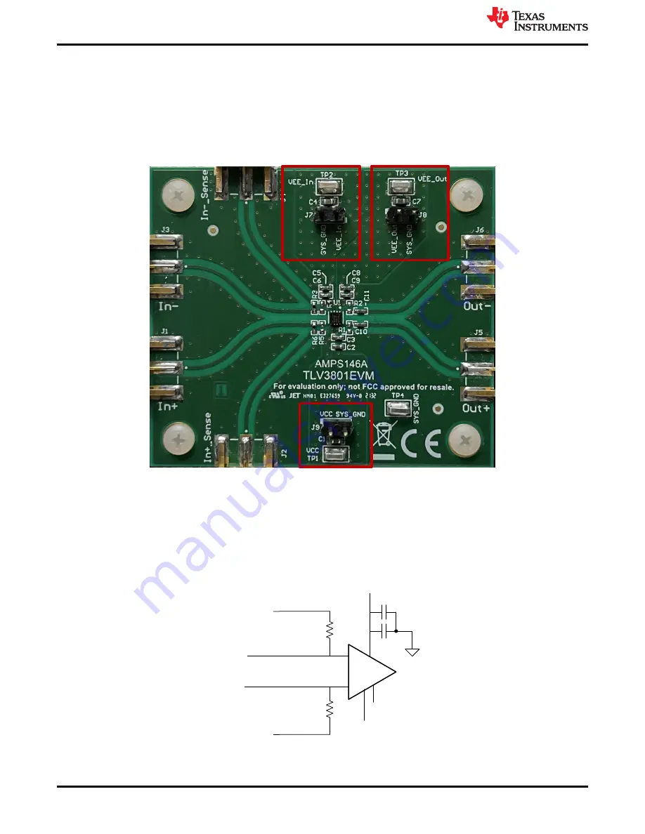
The TLV3801EVM can operate from a single supply or split supply configuration. If using the a single supply 
(VEE_In and VEE_Out shorted to GND), then the recommended voltage range is from 2.7-V to 5.5-V. When a 
split supply configuration is used, then VCC - VEE (applies to both VEE_In and VEE_Out) has a range of 2.7-V 
to 5.5-V and VCC - GND has a range of 2.4-V to 5.25-V. Connect VCC, VEE_In, and VEE_Out using TP1, TP2, 
and TP3 respectively.

Figure 6-1. TLV3801EVM Supply Voltage Connection

6.2 Inputs

Resistors R6 and R3 are 0-Ω resistors. The input terminals (IN+ and IN-) have corresponding sense lines so that 
the inputs to the device can be terminated on the lines with 50-Ω to an oscilloscope. This allows the input signals 
to be observed with minimal loading and distortion. There are also optional input resistors R4 and R5 for direct 
50-Ω terminations if required by the input signal generator, otherwise they can be left uninstalled.

R3 0

+

– 

R6 0

GND

IN+_SENSE

IN-_SENSE

V

CC

V

EE_Out

V

EE_In

IN+

IN-

Figure 6-2. Input Side Schematic Without Optional Resistors R4 and R5

Board Setup

www.ti.com

8

TLV3801EVM User’s Guide

SNOU184 – NOVEMBER 2021

Submit Document Feedback

Copyright © 2021 Texas Instruments Incorporated

Содержание TLV3801EVM

Страница 1: ...Schematic 12 9 Bill of Materials 13 List of Figures Figure 1 1 TLV3801EVM Board Top View 2 Figure 2 1 TLV3801 Block Diagram 3 Figure 3 1 TLV3801EVM Pin Assignments 4 Figure 3 2 How EVM Designations are Mapped to the TLV3801 Pinout 4 Figure 5 1 TLV3801 EVM Propagation Delay with Latch Setup 6 Figure 5 2 Quick Start Example 7 Figure 6 1 TLV3801EVM Supply Voltage Connection 8 Figure 6 2 Input Side Sc...

Страница 2: ...nce with different measurement tools The output of the TLV3801 is designed for low voltage differential signals LVDS which provide high speed signals to interconnect devices such as FPGAs with minimal power dissipation Figure 1 1 TLV3801EVM Board Top View Introduction www ti com 2 TLV3801EVM User s Guide SNOU184 NOVEMBER 2021 Submit Document Feedback Copyright 2021 Texas Instruments Incorporated ...

Страница 3: ... Detection Capability LVDS Output Low Input Offset Voltage DSG Package 8 pin WSON VCC VEE TLV3801 100 OUT IN IN OUT VCC LVDS GND Figure 2 1 TLV3801 Block Diagram www ti com Features SNOU184 NOVEMBER 2021 Submit Document Feedback TLV3801EVM User s Guide 3 Copyright 2021 Texas Instruments Incorporated ...

Страница 4: ... to the GND pin on the TLV3801 The difference between the VCC pin and the GND pin is the output supply voltage The recommended output supply voltage VCC GND range is 2 4 V to 5 25 V OUT OUT IN IN OUT OUT GND VEE VCC VCC IN IN 1 2 3 4 8 7 6 5 Thermal Pad VEE_Out VEE_In VCC Figure 3 2 How EVM Designations are Mapped to the TLV3801 Pinout When using a single supply VEE_In VEE pin and VEE_Out GND are ...

Страница 5: ...rminations SMA Cables adapters All sensed input voltages and both output signals must have matched cable lengths IN SENSE IN SENSE only if AC signal OUT and OUT All other signals can use non matched cable lengths www ti com Recommended Equipment SNOU184 NOVEMBER 2021 Submit Document Feedback TLV3801EVM User s Guide 5 Copyright 2021 Texas Instruments Incorporated ...

Страница 6: ...drive Disable the signal generator output Connect the signal generator output to IN 6 Ground the inverting input IN to ground to establish the threshold for the comparator at 0 V 7 Connect OUTP and OUTN to a 50 Ω terminated channel on the oscilloscope Note that with capacitors C10 and C11 populated the discharging and charging of these output capacitors will cause the output to be averaged 8 Conne...

Страница 7: ...eaches 0 V The propagation delay was measured at approximately 206 ps with the setup described Channel 4 OUT Channel 1 100mV peak to peak VOD 50mV VUD 50mV 10MHz Channel 3 OUT Figure 5 2 Quick Start Example www ti com How to Make a TPHL Propagation Delay Measurement With Split Supplies SNOU184 NOVEMBER 2021 Submit Document Feedback TLV3801EVM User s Guide 7 Copyright 2021 Texas Instruments Incorpo...

Страница 8: ... 2 Inputs Resistors R6 and R3 are 0 Ω resistors The input terminals IN and IN have corresponding sense lines so that the inputs to the device can be terminated on the lines with 50 Ω to an oscilloscope This allows the input signals to be observed with minimal loading and distortion There are also optional input resistors R4 and R5 for direct 50 Ω terminations if required by the input signal genera...

Страница 9: ...result in a DC portion of the signal that is not halfway between VOH and VOL As mentioned earlier this is because of the charging and discharging of the capacitors A higher duty cycle will result in a higher DC output voltage because the capacitors are charging more than they are discharging GND VCC VEE_Out C10 0 1uF C11 0 1uF OUT OUT Figure 6 4 Output Side Schematic If equipment is available to m...

Страница 10: ...nes Top Layer GND 1 Layer GND 2 Layer Bottom Layer Figure 7 1 Layers Layout Guidelines www ti com 10 TLV3801EVM User s Guide SNOU184 NOVEMBER 2021 Submit Document Feedback Copyright 2021 Texas Instruments Incorporated ...

Страница 11: ...D IN IN IN _SENSE IN _SENSE VCC VEE_Out VEE_In Figure 7 2 TLV3801 EVM Block Diagram www ti com Layout Guidelines SNOU184 NOVEMBER 2021 Submit Document Feedback TLV3801EVM User s Guide 11 Copyright 2021 Texas Instruments Incorporated ...

Страница 12: ...8 Schematic Figure 8 1 TLV3801 EVM Schematic Schematic www ti com 12 TLV3801EVM User s Guide SNOU184 NOVEMBER 2021 Submit Document Feedback Copyright 2021 Texas Instruments Incorporated ...

Страница 13: ...J6 6 SMA Connector Receptacle Female Socket 50Ohm Board Edge End Launch Solder 0732511150 Molex Inc J7 J8 J9 3 Header 100mil 2x1 Gold TH Header 2 54mm 2x1 TH HMTSW 102 07 G S 240 Samtec LBL1 1 Thermal Transfer Printable Labels 0 650 W x 0 200 H 10 000 per roll PCB Label 0 650 x 0 200 inch THT 14 423 10 Brady R3 R6 2 0 RES 0 0 0 2 W AEC Q200 Grade 0 0402 0402 CRCW04020000Z0EDHP Vishay Dale TP1 TP2 ...

Страница 14: ...other than TI b the nonconformity resulted from User s design specifications or instructions for such EVMs or improper system design or c User has not paid on time Testing and other quality control techniques are used to the extent TI deems necessary TI does not test all parameters of each EVM User s claims against TI under this Section 2 are void if User fails to notify TI of any apparent defects...

Страница 15: ... These limits are designed to provide reasonable protection against harmful interference in a residential installation This equipment generates uses and can radiate radio frequency energy and if not installed and used in accordance with the instructions may cause harmful interference to radio communications However there is no guarantee that interference will not occur in a particular installation...

Страница 16: ...y for convenience and should be verified by User 1 Use EVMs in a shielded room or any other test facility as defined in the notification 173 issued by Ministry of Internal Affairs and Communications on March 28 2006 based on Sub section 1 1 of Article 6 of the Ministry s Rule for Enforcement of Radio Law of Japan 2 Use EVMs only after User obtains the license of Test Radio Station as provided in R...

Страница 17: ... any interfaces electronic and or mechanical between the EVM and any human body are designed with suitable isolation and means to safely limit accessible leakage currents to minimize the risk of electrical shock hazard User assumes all responsibility and liability for any improper or unsafe handling or use of the EVM by User or its employees affiliates contractors or designees 4 4 User assumes all...

Страница 18: ...OR DAMAGES ARE CLAIMED THE EXISTENCE OF MORE THAN ONE CLAIM SHALL NOT ENLARGE OR EXTEND THIS LIMIT 9 Return Policy Except as otherwise provided TI does not offer any refunds returns or exchanges Furthermore no return of EVM s will be accepted if the package has been opened and no return of the EVM s will be accepted if they are damaged or otherwise not in a resalable condition If User feels it has...

Страница 19: ...o change without notice TI grants you permission to use these resources only for development of an application that uses the TI products described in the resource Other reproduction and display of these resources is prohibited No license is granted to any other TI intellectual property right or to any third party intellectual property right TI disclaims responsibility for and you will fully indemn...

Отзывы: