


Functional Description
707
SLAU723A – October 2017 – Revised October 2018
Copyright © 2017–2018, Texas Instruments Incorporated
Analog-to-Digital Converter (ADC)
Table 10-2. Sample and Hold Width in ADC
Clocks (continued)
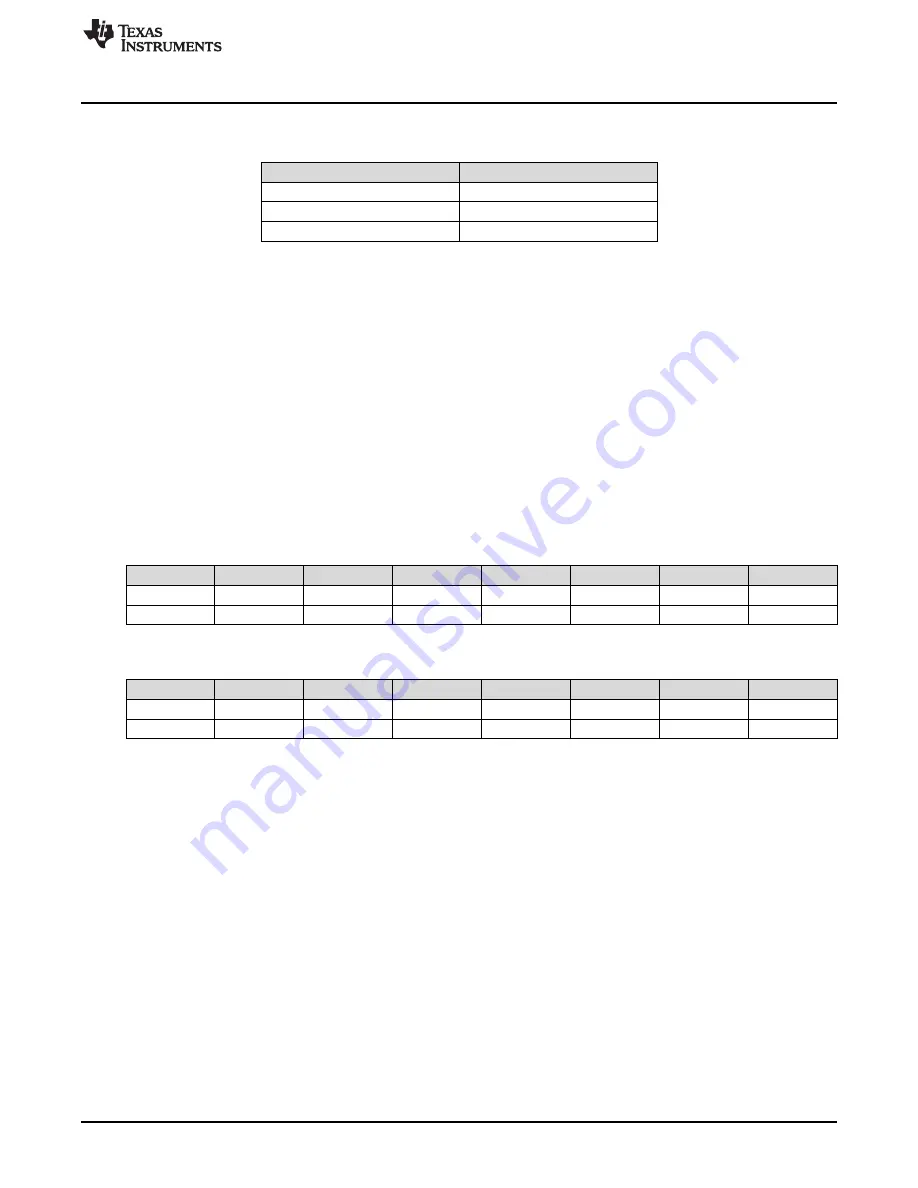
TSHn Encoding
N
SH
0xB
Reserved
0xC
256
0xD-0xF
Reserved
The ADC conversion frequency is a function of the Sample and Hold number, given by the following
equation:
f
CONV
= 1 / ((N
SH
+ 12) × T
ADC
)
where:
•
N
SH
is the sample and hold width in ADC clocks
•
T
ADC
is the ADC conversion clock period, which is the inverse of the ADC clock frequency f
ADC
Now, the maximum allowable external source resistance (R
S
) also changes with the value of N
SH
, as the
total settling time of the input circuitry must be fast enough to settle to within the ADC resolution in a
single sampling interval. The input circuitry includes the external source resistance as well as the input
resistance and capacitance of the ADC (R
ADC
and C
ADC
).
The values for R
S
and f
CONV
for varying N
SH
values, with f
ADC
= 16 MHz and f
ADC
= 32 MHz are given in
tables 18-4-a and 18-4-b. The system designer must take into consideration both of these factors for
optimal ADC operation.
Table 10-3. R
S
and f
CONV
Values with Varying N
SH
Values and f
ADC
= 16 MHz
N
SH
(Cycles)
4
8
16
32
64
128
256
f
CONV
(ksps)
1000
800
571
364
211
114
60
R
S
max (
Ω
)
500
3500
9500
21500
45500
93500
189500
Table 10-4. R
S
and f
CONV
Values with Varying N
SH
Values and f
ADC
= 32 MHz
N
SH
(Cycles)
4
8
16
32
64
128
256
f
CONV
(ksps)
2000
1600
1143
727
421
229
119
R
S
max (
Ω
)
250
500
3500
9500
21500
45500
93500
10.3.2.6 Sample Phase Control
The trigger source for ADC0 and ADC1 may be independent or the two ADC modules may operate from
the same trigger source and operate on the same or different inputs. If the converters are running at the
same sample rate, they may be configured to start the conversions coincidentally or one ADC may be
programmed to lag up to 15 clock cycles relative to the other ADC. The sample time can be delayed from
the standard sampling time by programming the PHASE field in the ADC Sample Phase Control
(ADCSPC) register.
shows an example of various phase relationships.


