Control Registers
283
SPNU503C – March 2018
Copyright © 2018, Texas Instruments Incorporated
F021 Flash Module Controller (FMC)
5.7.19 Flash Pump Access Control Register 2 (FPAC2)
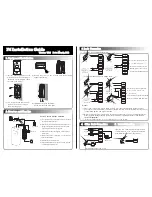
Figure 5-26. Flash Pump Access Control Register 2 (FPAC2) [offset = 4Ch]
31
16
Reserved
R-0
15
0
PAGP
R/WP-0
LEGEND: R/W = Read/Write; R = Read only; WP = Write in Privilege Mode; -
n
= value after reset
Table 5-31. Flash Pump Access Control Register 2 (FPAC2) Field Descriptions
Bit
Field
Value
Description
31-16
Reserved
0
Reads return 0. Writes have no effect.
15-0
PAGP
Pump Active Grace Period
This register contains the starting count value for the PAGP mode down counter. Any access to
Flash memory causes the counter to reload with the PAGP value. After the last access to Flash
memory, the down counter delays from 0 to 65535 prescaled HCLK clock cycles before entering
one of the charge pump fallback power modes as determined by PUMPPWR in the FPAC1 register.
Note:
The PAGP down counter is clocked by the same prescaled clock as the BAGP down counter
which is a divide by 16 of HCLK.
5.7.20 Flash Module Access Control Register (FMAC)
Figure 5-27. Flash Module Access Control Register (FMAC) [offset = 50h]
31
16
Reserved
R-0
15
3
2
0
Reserved
BANK
R-0
R/WP-0
LEGEND: R/W = Read/Write; R = Read only; WP = Write in Privilege Mode; -
n
= value after reset
Table 5-32. Flash Module Access Control Register (FMAC) Field Descriptions
Bit
Field
Value
Description
31-16
Reserved
0
Reads return 0. Writes have no effect.
2-0
BANK
Bank Enable.
These bits select which bank is enabled for operations such as local register access, OTP sector
access, and program/erase commands. These bits select only one bank at a time from up to eight
banks depending on the specific device being used. For example, a 000 selects bank 0; 011 selects
Bank 3.
Note:
BANK[2:0] can identify up to 8 Flash banks. If BANK[2:0] is selected for an unimplemented
bank then the BANK[2:0] will set itself to the number of an implemented bank. To determine if a
bank is implemented, write the bank number to BANK[2:0] and read back the value to see if what
was written can be read back.