


1
SNVU592D – July 2018 – Revised April 2020
Copyright © 2018–2020, Texas Instruments Incorporated
LM5180-Q1 Single-Output EVM User's Guide
User's Guide
SNVU592D – July 2018 – Revised April 2020
LM5180-Q1 Single-Output EVM User's Guide
With input voltage range and current capability as specified in
, the family of PSR flyback DC/DC
converters from TI provides flexibility, scalability, and optimized solution size for a range of applications.
Using an 8-pin WSON package with 4-mm × 4-mm footprint and 0.8-mm pin pitch, these converters
enable isolated DC/DC solutions with high density and low component count.
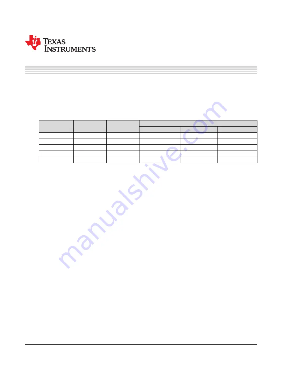
Table 1. PSR Flyback DC/DC Converter Family
PSR FLYBACK
CONVERTER
INPUT VOLTAGE
RANGE
PEAK SWITCH
CURRENT (TYP)
MAXIMUM LOAD CURRENT, V
OUT
= 12 V, N
PS
= 1
V
IN
= 4.5 V
V
IN
= 13.5 V
V
IN
= 24 V
4.5 V to 65 V
0.75 A
90 mA
180 mA
225 mA
4.5 V to 65 V
1.5 A
180 mA
360 mA
450 mA
4.5 V to 42 V
1.5 A
180 mA
360 mA
450 mA
4.5 V to 42 V
2.5 A
300 mA
600 mA
750 mA
4.5 V to 42 V
4.1 A
500 mA
1 A
1.25 A
The
evaluation module (EVM) is a flyback DC/DC converter that employs primary-side
regulation (PSR) based on sampling of the primary winding voltage of the transformer to achieve high
efficiency in a small footprint. It operates over a wide input voltage range of 10 V to 65 V, providing a
regulated 5-V output using a transformer with 3 : 1 turns ratio. Operating without an optocoupler or
transformer auxiliary winding, the converter delivers an output voltage with ±1.5% regulation.
The EVM design uses the
65-V PSR flyback converter. An integrated 100-V, 1.5-A power
MOSFET provides ample margin for line transients and switch (SW) node voltage spikes related to
transformer parasitic leakage inductance. Load regulation errors related to transformer secondary winding
resistance are avoided by virtue of the quasi-resonant boundary conduction mode (BCM) control scheme.
Additional features includes current-mode control with internal compensation, hiccup-mode fault
protection, programmable soft-start, and optional output voltage temperature compensation. Input UVLO
protects the converter at low input voltage conditions, and the EN/UVLO pin supports adjustable UVLO
with user-defined hysteresis for application specific power-up and power-down requirements.
The LM(2)5180 and LM(2)5180-Q1 converters are available in a 8-pin WSON package with 4-mm × 4-mm
footprint and 0.8-mm pin pitch to enable isolated DC/DC solutions with high density and low component
count. Wettable flank pins provide a visual indicator of solderability, which reduces inspection time and
manufacturing costs in high-reliability industrial and automotive applications. See the
and
data sheets for more information. Use the LM5180-Q1 with
to
create a custom regulator design. Furthermore, you can download the
to
optimize component values and examine predicted efficiency performance across line and load ranges.
Contents
1
High Density EVM Description
.............................................................................................
1.1
Typical Applications
................................................................................................
1.2
Features and Electrical Performance
............................................................................
2
EVM Performance Characteristics
.........................................................................................
3
Application Circuit Diagram
.................................................................................................
4
EVM Photo
....................................................................................................................
5
Test Setup and Procedure
..................................................................................................
5.1
Test Setup
...........................................................................................................
5.2
Test Equipment
.....................................................................................................
5.3
Recommended Test Setup
........................................................................................


