Texas Instruments DRV8328 EVM Series Скачать руководство пользователя страница 9

Table 3-2. Description of user selectable settings on DRV8328AEVM (continued)

Id.

Setting Name

Description

Position

Function

I

DRVOFF switch

Turns off the gate driver 
outputs.

S2 = Down

Drivers are on

S2 = Up

Drivers are off (DRVOFF 
is enabled)

J

Phase voltage feedback

Resistor divider and 
filtering capacitor for 
phase voltage feedback to 
MCU ADCs.

R67, R70, C45

Phase A voltage feedback

R68, R71, C46

Phase B voltage feedback

R69, R72, C47

Phase C voltage feedback

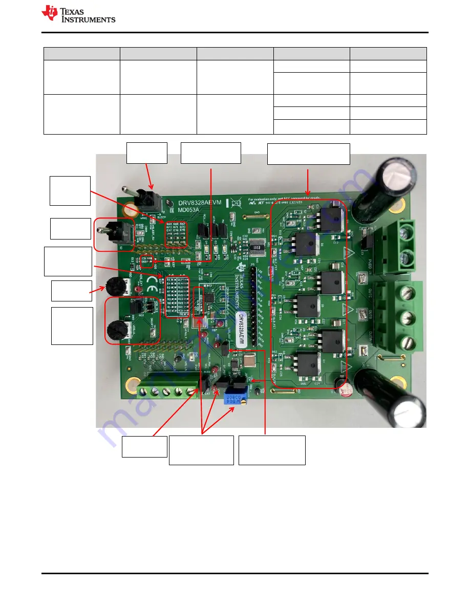
(C) Power stage MOSFETs  

and passive components

(G) VDSLVL  
pot, select,  

and disable  

jumpers

(F) Hall  

Power select

(E) Dead 

me  

poten ometer,  

jumper, & resistor

(I) DRVOFF  

switch

(A) nSLEEP  

switch

(B) External CSA  

output 

lter

(H) DRV8328  

A/B or C/D  

select  

(D) LDO enable and  

LDO output enable  

jumpers

(J) Phase  

voltage  

feedback

(K) Speed  

pot

Figure 3-6. User-adjustable jumpers, resistors, and switches on DRV8328AEVM

3.4.1 DRV8328A/B Compatibility

The DRV8328AEVM default is the DRV8328A (Hardware variant), but can also be compatible with the 
DRV8328B. The main difference is that DRV8328A operates in 6x PWM mode and DRV8328B operates in 3x 
PWM mode. 

Figure 3-7

 shows the default resistors to select the A/B variant when the DRV8328A or DRV8328B 

is used. Ensure resistors R1-R10 are removed, C1 is removed, and resistors R11-R21 are populated (except 
R16).

www.ti.com

Hardware and Software Overview

SLVUCD3A – NOVEMBER 2021 – REVISED AUGUST 2022

Submit Document Feedback

DRV8328xEVM User's Guide

9

Copyright © 2022 Texas Instruments Incorporated

Содержание DRV8328 EVM Series

Страница 1: ...onnections Overview DRV8328AEVM LAUNCHXL F280049C 4 3 2 Connection Details 4 3 3 LED Lights 6 3 4 DRV8328AEVM Configurability and Switch Functions 7 3 5 Interfacing DRV8328AEVM and LAUNCHXL F280049C L...

Страница 2: ...iptions default of EVM in bold Device Name LDO Output DT pin and VDSLVL pin PWM Mode DRV8328A N A Available 6x PWM DRV8328B N A Available 3x PWM DRV8328C 3 3 V N A 6x PWM DRV8328D 3 3 V N A 3x PWM The...

Страница 3: ...all sensors to the appropriate locations on the 5 pin connector J10 as shown in Figure 3 2 Select AVDD or EXT on jumper J11 to choose the Hall power source voltage 3 Mate the DRV8328AEVM onto the top...

Страница 4: ...3 2 shows the power supply and motor connections made to the DRV8328AEVM in order to spin a 3 phase sensored or sensorless Brushless DC motor A 4 5 V to 60 V power supply or battery is connected to t...

Страница 5: ...o the LAUNCHXL F280049C to provide communication between the LaunchPad firmware and GUI as well as the correct installment of the DRV8328AEVM to the J1 J3 and J2 J4 headers of the LaunchPad www ti com...

Страница 6: ...EVM has 4 status LEDs on the board By default the PVDD and AVDD LEDs will light up when the board is powered on The fault LED will light up when the driver reports a fault and the MCU LED tied to GPIO...

Страница 7: ...D LED Figure 3 5 DRV8328AEVM LEDs 3 4 DRV8328AEVM Configurability and Switch Functions The DRV8328AEVM includes a variety of user selectable jumpers and unpopulated components on the PCB to choose use...

Страница 8: ...Dead time potentiometer jumper resistor Jumper to enable dead time control from potentiometer and potentiometer used to set the resistance for DT pin DRV8328A B only J14 Populated DT from pot is enabl...

Страница 9: ...h B External CSA output lter H DRV8328 A B or C D select D LDO enable and LDO output enable jumpers J Phase voltage feedback K Speed pot Figure 3 6 User adjustable jumpers resistors and switches on DR...

Страница 10: ...ants are properly configured for their functions The DRV8328C and DRV8328D device remove the VDSLVL and dead time pins and are replaced with a DRVOFF shutdown pin and LDO AVDD The main difference betw...

Страница 11: ...appropriately to receive the functionalities of the DRV8328 device These 40 pins are grouped into 4 ports in respect to the LAUNCHXL F280049C J1 to J4 Table 3 5 and Table 3 6 list the interfacing of t...

Страница 12: ...r DRV8328AEVM Function LAUNCHXL F280049C Function Description 1 INHA GPIO10 PWM6A PWM used to switch Phase A High side FET 2 GND GND GND connection 3 INLA GPIO11 PWM6B PWM used to switch Phase A Low s...

Страница 13: ...GPIO59 Hall sensor C from motor Note There are many resistors that are not populated for internal use only Ensure the correct resistors are populated so every has signal has only signal path If multi...

Страница 14: ...UNCHXL F280049C The motor and power connectors should face to the LaunchPad s Micro USB connector 3 Connect the three phases from the brushless DC motor to the 3 pin connector J12 on DRV8328AEVM Phase...

Страница 15: ...8328DEVM GUI To access the GUIs please visit https dev ti com gallery search drv8328 You must register a TI account in order to access the Gallery 5 1 Connecting to the DRV8328xEVM GUI Follow the inst...

Страница 16: ...ould appear when the GUI is connected Direction Enabled PWM Frequency Hz 20000 MCU Dead Time ns 0 Acceleration Delay ms 1 duty cycle 21 Firmware and GUI Application www ti com 16 DRV8328xEVM User s Gu...

Страница 17: ...ontrol the speed of the motor If you do not wish to use the potentiometer skip this step 5 Turn the potentiometer clockwise or adjust the Duty Cycle slider to control the speed of the motor from 0 to...

Страница 18: ...tion Delay Sets the acceleration and deceleration ramp rate in ms per 1 duty cycle MOTOR BRAKING SETTINGS Stop Motor Stops the motor when toggled according to the braking method in the drop down menu...

Страница 19: ...A 20 I NHB 19 I NHC 18 I NLA 23 I NLB 22 I NLC 21 LSS 17 SHA 6 SHB 10 SHC 14 VDSLVL 26 GND 28 PowerPAD 29 DRV8328ARUYR U1 50V 1uF C3 50V 1uF C8 50V 1uF C9 50V 10 F C7 470nF 25V C6 nSLEEP nFAULT Place...

Страница 20: ...9C CSAREF nSLEEP_49C nFAULT_DFLT nSLEEP_DFLT LAUNCHXL F28069M LAUNCHXL F28027F EK TM4C123GXL and MSPM0G350x microcontrollers Figure 6 4 LaunchPad Connectors and Connections schematic 0 R26 0 R27 DNP n...

Страница 21: ...V C32 DNP 330pF 100V C28 DNP 50V 0 01uF C30 DNP GND GND 0 R58 0 R61 GND External C_GS capacitors can be replaced with 0 001 R60 k ohm pull down resistors if desired GND GND GND SN 1 3 4 CSD18536KTTT Q...

Страница 22: ...ad 160 ns DRV8328B or 55 ns DRV8328A R88 ohms t_Dead ns 200 10000 2 1 3 S1 nSLEEP_SW 10 0k R73 TP23 PVDD 3 3V 300mW D11 GND nSLEEP nSLEEP switch C36 R77 designed for 10us nSLEEP reset pulse MCU GPIO s...

Страница 23: ...TA OUTB OUTC CTAP 1 00k R78 DNP Depopulate R65 to disconnect CTAP from LP 4 99k R66 4 99k R70 110k R65 110k R69 110k R68 110k R67 4 99k R71 4 99k R72 4 99k R86 DNP 110k R83 DNP Figure 6 11 Voltage Sen...

Страница 24: ...ther than TI b the nonconformity resulted from User s design specifications or instructions for such EVMs or improper system design or c User has not paid on time Testing and other quality control tec...

Страница 25: ...These limits are designed to provide reasonable protection against harmful interference in a residential installation This equipment generates uses and can radiate radio frequency energy and if not in...

Страница 26: ...instructions set forth by Radio Law of Japan which includes but is not limited to the instructions below with respect to EVMs which for the avoidance of doubt are stated strictly for convenience and s...

Страница 27: ...any interfaces electronic and or mechanical between the EVM and any human body are designed with suitable isolation and means to safely limit accessible leakage currents to minimize the risk of electr...

Страница 28: ...R DAMAGES ARE CLAIMED THE EXISTENCE OF MORE THAN ONE CLAIM SHALL NOT ENLARGE OR EXTEND THIS LIMIT 9 Return Policy Except as otherwise provided TI does not offer any refunds returns or exchanges Furthe...

Страница 29: ...change without notice TI grants you permission to use these resources only for development of an application that uses the TI products described in the resource Other reproduction and display of thes...

Отзывы: