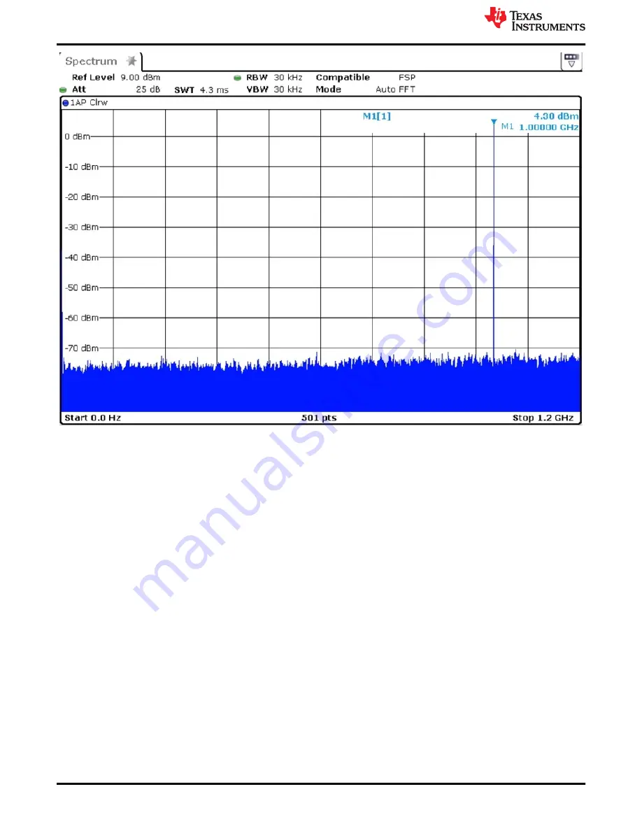
Figure 3-10. DAC Channel A Output
Setup Procedure
www.ti.com
16
DAC12DL3200 Evaluation Module
SBAU374 – MAY 2021
Submit Document Feedback
Copyright © 2021 Texas Instruments Incorporated
Страница 1: ...Program the DAC and Clocks for Single Channel NRZ Mode 2 Operation 9 3 10 Open the HSDC Software and Load the FPGA Image to the TSW14DL3200EVM 11 3 11 DxSTRB Timing Adjustment 14 4 Other Modes of Ope...
Страница 2: ...Nyquist output modes The DAC12DL3200EVM device input data is transmitted over a high speed LVDS interface This evaluation board also includes the following important features Transformer coupled outpu...
Страница 3: ...the DAC12DL3200 contributes approximately 6 ns of latency see the data sheet spec while the ADC12DL3200 adds a latency of approximately 8 ns The remaining delay is from the FPGA logic used FPGA DAC12D...
Страница 4: ...SW14DL3200EVM and ADC12DL3200EVM Operation Refer to the TSW14DL3200EVM User s Guide and ADC12DL3200EVM User s Guide for configuration and status information 2 Equipment This section describes the equi...
Страница 5: ...generators for clock inputs TI recommends the following Rohde Schwarz SMA100A or SMA100B Spectrum Analyzer Rohde Schwarz FSQ with 20 GHz of bandwidth or equivalent Signal path cables SMA to SMA 12 V D...
Страница 6: ...ure 3 1 shows the EVM test setup 12 V DC 5 V DC CHA OUT USB 3 0 DAC CLK LMK CLK USB Figure 3 1 EVM Test Setup Note The HSDC Pro software must be installed before connecting the TSW14DL3200EVM to the P...
Страница 7: ...2 4 5 7 8 10 11 13 14 16 17 Default is all inputs tied to GND J5 J7 J12 FTDI Spare GPIOs No shunt Default is all inputs disconnected These jumpers allow for FTDI to control NCO select inputs when inst...
Страница 8: ...Connect to the PC Use the following steps to turn on the TSW14DL3200EVM with 12 V power and connect to the PC 1 Turn on the 12 V power supply connected to the TSW14DL3200EVM 2 Connect a mini USB 3 0...
Страница 9: ...28 and LMX2592 The register map for each device is provided in the device data sheets Figure 3 2 illustrates the DAC12DL3200EVM GUI showing the USB status is connected to a PC Figure 3 2 Configuration...
Страница 10: ...see Figure 3 4 Figure 3 4 Selecting Configuration File This configuration file sets up the DAC to operate in a single channel mode with the output available only on CHA The same output is available o...
Страница 11: ...ber for the one connected to the DAC12DL3200EVM When the EVM powers up there is no firmware loaded in the FPGA Click the OK button on the No firmware Please select a device to load firmware into the b...
Страница 12: ...D1 D5 also illuminate 4 In the top middle of the GUI enter 6 4G for the Data Rate 5 Set the tone center 1GHz in the I Q Multitone Generator window in the lower left of the GUI 6 Enter the of tones 1...
Страница 13: ...p looks as shown in Figure 3 7 Figure 3 7 HSDC Pro GUI Setup www ti com Setup Procedure SBAU374 MAY 2021 Submit Document Feedback DAC12DL3200 Evaluation Module 13 Copyright 2021 Texas Instruments Inco...
Страница 14: ...in the top left of the DAC main page b Click on IO Delay Figure 3 8 IO Delay c Click the Debug Features button d Enter x10000004 for the Reg Address and x8000 for the Data in the Write section as show...
Страница 15: ...VM is powered down or firmware is reloaded these steps must be repeated e In the HSDC Pro GUI main page click the Send button in the upper left to send the test tone to the DAC EVM f There should now...
Страница 16: ...Figure 3 10 DAC Channel A Output Setup Procedure www ti com 16 DAC12DL3200 Evaluation Module SBAU374 MAY 2021 Submit Document Feedback Copyright 2021 Texas Instruments Incorporated...
Страница 17: ...This configuration file will setup the DAC to operate in dual channel mode with outputs available on CHA and CHB 5 In the HSDC Pro GUI in the device drop down menu select DAC12DL3200_MODE0_12b_sync_is...
Страница 18: ...DAC RESET switch 3 Click on the DAC12DL3200EVM Low Level View tab 4 Click on the File icon and navigate to EXT_CLK_Mode0_2xRF_Dual_DAC cfg and click the OK button to load the LMK and DAC registers Thi...
Страница 19: ...not required To enter the desired NCO frequency and phase settings the user must first enter the DAC sample rate in the box labeled as F_DACA MHz The value entered is in megahertz The user then selec...
Страница 20: ...If using the SPI_SYNC for the NCO SYNC source after making any changes to the NCO settings click on the SPI_SYNC button twice to synchronize the two NCOs Figure 4 3 NCOA Calculation Other Modes of Ope...
Страница 21: ...address and data value that was written to the DAC12DL3200 LMK04828 or LMX2592 This log file information can be saved by first highlighting the register settings to be saved then double clicking insid...
Страница 22: ...UT DACA DACB IOTEST_ALARM and DIE ID and FUSE configuration tabs Control of the LMK0428 device features are available in the PLL1 Configuration PLL2 Configuration SYSREF and SYNC and Clock Outputs con...
Страница 23: ...the Read Data field Can be used to synchronize the GUI with the state of the hardware Read all button Read from all registers in the Register Map summary and display the current state of the hardware...
Страница 24: ...n the EVM is connected to the PC Verify that the green USB Status LED light in the top right corner of the GUI is lit If it is not lit click the Reconnect FTDI button Close and start the configuration...
Страница 25: ...ng the LMK_100M_LMX_6400M_Mode2_NRZ_Single_DAC cfg configuration file the LMK04828 provides a 100 MHz reference clock to the LMX2592 a 50 MHz SYSREF clock to the DAC and a 400 MHz reference clock to t...
Страница 26: ...the GUI has this clock disabled Click on the LMX2592 tab and uncheck the OUTB PD box There is now a 6 4 GHz tone on SMB connector J20 LMX OUT Figure B 2 Default Board Clock Configuration Circuit Exter...
Страница 27: ...ther than TI b the nonconformity resulted from User s design specifications or instructions for such EVMs or improper system design or c User has not paid on time Testing and other quality control tec...
Страница 28: ...These limits are designed to provide reasonable protection against harmful interference in a residential installation This equipment generates uses and can radiate radio frequency energy and if not in...
Страница 29: ...instructions set forth by Radio Law of Japan which includes but is not limited to the instructions below with respect to EVMs which for the avoidance of doubt are stated strictly for convenience and s...
Страница 30: ...any interfaces electronic and or mechanical between the EVM and any human body are designed with suitable isolation and means to safely limit accessible leakage currents to minimize the risk of electr...
Страница 31: ...R DAMAGES ARE CLAIMED THE EXISTENCE OF MORE THAN ONE CLAIM SHALL NOT ENLARGE OR EXTEND THIS LIMIT 9 Return Policy Except as otherwise provided TI does not offer any refunds returns or exchanges Furthe...
Страница 32: ...are subject to change without notice TI grants you permission to use these resources only for development of an application that uses the TI products described in the resource Other reproduction and...