background image

www.ti.com

Bill of Materials and Board Layout

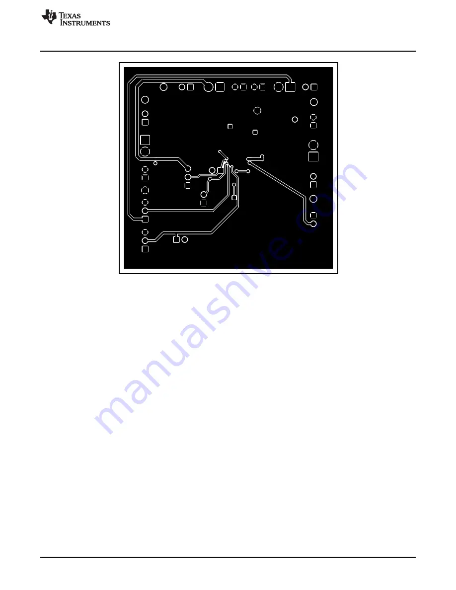
Figure 15. EVM PCB Bottom Layer

19

SLUUAA7A – July 2013 – Revised August 2014

User's Guide for bq25570 Battery Charger Evaluation Module for Energy

Harvesting

Submit Documentation Feedback

Copyright © 2013–2014, Texas Instruments Incorporated

Содержание bq25570

Страница 1: ...st and Measurment Summary 7 3 1 Test Setups and Results 8 4 Bill of Materials and Board Layout 17 4 1 Bill of Materials 17 4 2 EVM Board Layout 18 5 PCB Layout Guideline 20 List of Figures 1 EVM Schematic 4 2 Test Setup for Measuring Boost Charger Efficiency 9 3 Charger Efficiency versus Input Voltage 9 4 Charger Efficiency versus Input Current 10 5 Test Setup for Measuring Buck Converter Efficien...

Страница 2: ...he VOUT pin The VOUT voltage is externally programmed to slightly less than the VSTOR voltage HiZ DC sources have a maximum output power point MPP that varies with ambient conditions For example a solar panel s MPP varies with the amount of light on the panel and with temperature The MPP is listed by the harvesting source manufacturer as a percentage of its open circuit OC voltage Therefore the bq...

Страница 3: ...ing the data sheet first will help in understanding the operations and features of this IC In this document battery or VBAT will be used but one could substitute any appropriate storage element System Design Tips Compared to designing systems powered from an AC DC converter or large battery for example low impedance sources designing systems powered by HiZ sources requires that the system load per...

Страница 4: ...7 C3 22uF J11 JP2 JP3 L2 10 uH L1 22uH J6 J7 J9 J10 J12 R5 4 99M J1 J3 C9 C8 C10 1 VSS 2 VIN_DC 3 VOC_SAMP 4 VREF_SAMP 5 EN 6 VOUT_EN 7 VBAT_OV 8 VRDIV 9 NC 10 OK_HYST 11 OK_PROG 12 VOUT_SET 13 VBAT_OK 14 VOUT 15 VSS 16 LBUCK 17 NC 18 VBAT 19 VSTOR 20 LBOOST 21 PWPD U1 BQ25570RGR BQ25570RGR TP3 TP6 TP8 TP9 JP6 VIN1 VIN1 VSTOR VOC_SAMP VBAT VSTOR VOC_SAMP VBAT VRDIV VRDIV Introduction www ti com 1 ...

Страница 5: ...converter output terminal block J12 GND Buck converter output J13 BAT_OK Battery Status Indicator Test Points TP1 Input source TP2 Boost charger switching node TP3 Buck converter switching node TP4 Boost charger output VSTOR TP5 Rechargeable storage element connection BAT_SEC TP6 Buck converter output VOUT TP7 VRDIV node CAUTION Providing an additional low impedance current path in parallel with t...

Страница 6: ...ding an additional leakage path for the VREF_SAMP capacitor for example GND through a 10 MΩ scope probe attached to VREF_SAMP will degrade input voltage regulation performance JP6 VBAT_OK to BAT_OK VOUT_EN configures the buck converter to be Uninstalled NOTE Do not install if JP3 shunt is installed VOUT_EN enabled only when VSTOR is greater than the VBAT_OK threshold per the resistors 2 786V on th...

Страница 7: ...r flux on a board has a resistivity in the 1 20 MΩ range Therefore flux remaining in parallel with changed 1 20 MΩ resistors can result in a lower effective resistances which will produce different operating thresholds than expected Similarly flux remaining in parallel with the VREF_SAMP capacitor provides an additional leakage path which results in the input voltage regulation set point drooping ...

Страница 8: ...attery and a lab supply connected to the BAT pin via a diode The lab supply biases up the battery voltage to the desired level It may be necessary to add more capacitance across R1 3 1 Test Setups and Results 3 1 1 Boost Charger Efficiency The test setup is shown in Figure 2 The specific equipment used for the test results in Figure 3 and Figure 4 is listed below 1 VIN_DC was connected to a Keithl...

Страница 9: ...SM1 SM1 Source Sink Meter Configured As Voltage Source SM2 SM2 www ti com Test and Measurment Summary Figure 2 Test Setup for Measuring Boost Charger Efficiency Figure 3 Charger Efficiency versus Input Voltage 9 SLUUAA7A July 2013 Revised August 2014 User s Guide for bq25570 Battery Charger Evaluation Module for Energy Harvesting Submit Documentation Feedback Copyright 2013 2014 Texas Instruments ...

Страница 10: ...input regulation loop may interfere with each other and cause the input voltage to oscillate Adding a large capacitor across VIN_DC and GND will eliminate this oscillation but the capacitor s leakage current will inflate the input current measurement and result in lower efficiency See SLUA691 for a detailed explanation on how to take these and other measurements with source meters 3 1 2 Buck Conve...

Страница 11: ...rom the VSTOR supply must be set to the highest level of filtering and or averaging which will result in longer than usual measurement times Alternatively these measurements can be taken with source meters instead of discrete power supply resistor load box and meters The source meter on VSTOR is configured as a voltage source The source meter on OUT can be configured as either a current source tha...

Страница 12: ...with a series resistor that switches in a 36 Ω resistor 3 VBAT was connected a 3 2 V charged 4 2 V coin cell 4 VSTOR VOUT and VIN_DC was monitored by oscilloscope voltage scope probes attached to TP4 TP6 and TP1 respectively and GND IOUT was measured with a current probe Figure 7 Test Setup for Performing Load Transient on Buck Output Figure 8 50 mA Load Transient on VOUT 12 User s Guide for bq255...

Страница 13: ...ith inductor L1 3 VSTOR s ripple voltage was measured using an oscilloscope voltage probe placed directly across the VSTOR capacitor C5 The scope probe s standard ground lead was replaced with very short lead 4 VIN and the LBOOST pin switching node of the boost charger were measured by oscilloscope voltage probes connected to TP1 and TP2 Figure 9 Charger Operational Waveforms During 50 mA Load Tra...

Страница 14: ...using an oscilloscope voltage probe placed directly across the VSTOR capacitor C5 VOUT s ripple voltage was measured using an oscilloscope voltage probe placed directly across the VOUT capacitor C3 Both scope probes standard ground leads were replaced with very short lead 4 The LBUCK pin s ripple voltage switching node of the buck converter was measured by a oscilloscope voltage probe connected to...

Страница 15: ...loads on VSTOR VBAT or VOUT 3 VIN_DC VSTOR and VOUT were measured with oscilloscope voltage probes connected at TP1 TP4 and TP6 Figure 11 Test Setup for Charging a Super Capacitor from Buck Output Figure 12 Charging a Super Cap from VOUT The benefit of charging of the super capacitor on VOUT instead of VBAT is faster charge time due to the charger spending less time in less efficient cold start mo...

Страница 16: ...istor to the ground of the EVM A 10 MΩ meter can be used to measure the voltage drop across the resistor and calculate the current No other connections should be made to the EVM and the measurement should be taken after steady state conditions are reached may take a few minutes The reading should be much less than 100 nA 16 User s Guide for bq25570 Battery Charger Evaluation Module for Energy SLUU...

Страница 17: ...mm 744031220 1 L2 10 uH Inductor SMT 1 4A 216mΩ 2 0mm x 2 5 mm 1239AS H 100N Toko Inductor SMT 250mA 500mΩ 2 5mm x 2 0mm x 1 00mm 74479888310 Wurth Elektronik Inductor SMT 500mA 390mΩ 2 8mm x 2 8mm x 1 35mm 744029100 Wurth Elektronik Inductor SMT 500mA 500mΩ 2 5mm x 2 0mm x 1 2mm 74479889310 Wurth Elektronik 1 R1 7 5M Resistor Chip 1 16W 1 603 CRCW06037M50FKEA Vishay Dale 1 R10 8 66M Resistor Chip...

Страница 18: ... L1 L2 R1 R10 R2 R3 R4 R5 R6 R7 R8 R9 TP1 TP4 TP5 TP6 TP2 TP3 TP7 TP8 TP9 U1 Bill of Materials and Board Layout www ti com 4 2 EVM Board Layout Figure 13 through Figure 15 are the board layouts for this EVM Figure 13 EVM PCB Top Assembly Figure 14 EVM PCB Top Layer 18 User s Guide for bq25570 Battery Charger Evaluation Module for Energy SLUUAA7A July 2013 Revised August 2014 Harvesting Submit Docu...

Страница 19: ...Layout Figure 15 EVM PCB Bottom Layer 19 SLUUAA7A July 2013 Revised August 2014 User s Guide for bq25570 Battery Charger Evaluation Module for Energy Harvesting Submit Documentation Feedback Copyright 2013 2014 Texas Instruments Incorporated ...

Страница 20: ...und return paths for example from resistors and CREF it is recommended to use short traces as well separated from the power ground traces and connected to VSS pin 15 This avoids ground shift problems which can occur due to superimposition of power ground current and control ground current The PowerPad should not be used as a power ground return path The remaining pins are either NC pins that shoul...

Страница 21: ...ndling and use of EVMs and if applicable compliance in all respects with such laws and regulations 10 User has sole responsibility to ensure the safety of any activities to be conducted by it and its employees affiliates contractors or designees with respect to handling and using EVMs Further user is responsible to ensure that any interfaces electronic and or mechanical between EVMs and any human ...

Страница 22: ...This equipment generates uses and can radiate radio frequency energy and if not installed and used in accordance with the instruction manual may cause harmful interference to radio communications Operation of this equipment in a residential area is likely to cause harmful interference in which case the user will be required to correct the interference at its own expense FCC Interference Statement ...

Страница 23: ...érieur au gain maximal indiqué sont strictement interdits pour l exploitation de l émetteur Mailing Address Texas Instruments Post Office Box 655303 Dallas Texas 75265 Copyright 2014 Texas Instruments Incorporated spacer Important Notice for Users of EVMs Considered Radio Frequency Products in Japan EVMs entering Japan are NOT certified by TI as conforming to Technical Regulations of Radio Law of ...

Страница 24: ...esponsible for compliance with all legal regulatory and safety related requirements concerning its products and any use of TI components in its applications notwithstanding any applications related information or support that may be provided by TI Buyer represents and agrees that it has all the necessary expertise to create and implement safeguards which anticipate dangerous consequences of failur...

Отзывы: