background image

www.ti.com

Bill of Materials and Board Layout

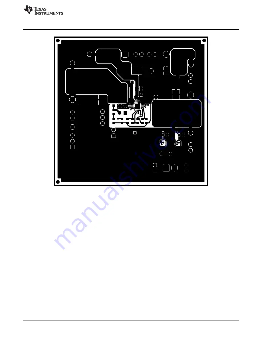
Figure 13. EVM PCB Top Layer

17

SLUUAA8 – September 2013

User's Guide for bq25505 Battery Charger Evaluation Module for Energy

Harvesting

Submit Documentation Feedback

Copyright © 2013, Texas Instruments Incorporated

Содержание bq25505

Страница 1: ...ance Specification Summary 7 3 Test and Measurement Summary 7 3 1 Test Setups and Results 8 4 Bill of Materials and Board Layout 14 4 1 Bill of Materials 14 4 2 EVM Board Layout 15 5 PCB Layout Guideline 19 List of Figures 1 bq25505EVM Schematic 4 2 Test Setup for Measuring Boost Charger Efficiency 8 3 Charger Efficiency versus Input Voltage 9 4 Charger Efficiency versus Input Current 9 5 Test Set...

Страница 2: ...ower point MPP that varies with ambient conditions For example a solar panel s MPP varies with the amount of light on the panel and with temperature The MPP is listed by the harvesting source manufacturer as a percentage of its open circuit OC voltage Therefore the bq25505 implements a programmable maximum power point tracking MPPT sampling network to optimize the transfer of power into the device...

Страница 3: ...ing the operations and features of this IC In this document secondary rechargeable battery or VBAT_SEC will be used but one could substitute any appropriate storage element System Design Tips Compared to designing systems powered from an AC DC converter or large battery for example low impedance sources designing systems powered by Hi Z sources requires that the system load per unit time for examp...

Страница 4: ...R5 4 99M J1 J3 C9 DNP C7 DNP J15 J14 J16 C8 DNP 1 VSS 2 VIN_DC 3 VOC_SAMP 4 VREF_SAMP 5 EN 6 NC 7 VBAT_OV 8 VRDIV 9 VB_SEC_ON 10 VB_PRI_ON 11 OK_HYST 12 OK_PROG 13 VBAT_OK 14 VBAT_PRI 15 VSS 16 NC 17 NC 18 VBAT_SEC 19 VSTOR 20 LBOOST 21 PWPD U1 BQ25505RGR TP6 TP8 TP3 C10 4 7uF VIN1 VIN1 VB_PRI_ON VBAT_PRI VSTOR VOC_SAMP BAT_SEC VB_SEC_ON VSTOR VB_PRI_ON VOC_SAMP BAT_SEC VBAT_PRI VRDIV VRDIV VB_SEC...

Страница 5: ...connection VBAT_PRI is an optional non rechargeable battery that switches in to the power the system when BAT_SEC drops below the VBAT_OK threshold J11 Non rechargeable storage element connection terminal VBAT_PRI GND block J12 GND Non rechargeable storage element connection return J13 BAT_OK GND Battery Status Indicator J14 VOR Output of multiplexing switches either VSTOR or VBAT_PRI J15 VOR GND ...

Страница 6: ... VREF_SAMP VREF_SAMP GND Uninstalled NOTE Providing an additional leakage path for the VREF_SAMP capacitor for example to GND through a 10 MΩ scope probe attached to VREF_SAMP will degrade input voltage regulation performance JP4 VOC_SAMP VOC_SAMP 80 configures the IC to regulate VIN to JP4 80 NOTE Do not install if JP1 shunt is installed 80 of VIN_OC VOC_SAMP 50 configures the IC to regulate VIN ...

Страница 7: ...removing the old components and again after installing the new components If possible the boards should be cleaned until the wash solution measures ionic contamination greater than 50 MΩ 3 Test and Measurement Summary Test Setup Tips Energy harvesting power sources are high impedance sources A source meter configured as a current source with voltage compliance set to the harvester s open circuit v...

Страница 8: ...red as a current source with voltage compliance clamp set to the open circuit voltage 2 VSTOR was connected a Keithley 2420 source meter configured as a voltage source set to the VSTOR voltage The current sunk by the source meter was the output current of the charger 3 VREF_SAMP was connected to a power supply configured to output the desired input voltage regulation point that is the MPPT times t...

Страница 9: ...veraging which will result in longer than usual measurement times but not longer than the 16 s MPPT sample time Measurements for both VIN and IN will be most accurate when taken at the midpoint of the 16 s MPPT period Remote sensing by the source meters is possible but on the input side the source meter output regulation loop and the charger MPPT input regulation loop may interfere with each other...

Страница 10: ...rt lead 4 VIN_DC and the LBOOST pin switching node of the boost charger were measured by oscilloscope voltage probes connected to TP1 and TP2 Figure 5 Test Setup for Measuring Charger Operation Figure 6 Charger Operational Waveforms During Battery Charging 10 User s Guide for bq25505 Battery Charger Evaluation Module for Energy SLUUAA8 September 2013 Harvesting Submit Documentation Feedback Copyri...

Страница 11: ...SEC and VBAT_PRI are configured as shown in Section 3 1 2 2 The function generator and power amplifier simulated VSTOR charging up and discharging 3 VBAT_SEC VBAT_PRI VBAT_OK and VOR were measured with oscilloscope voltage probes at TP5 TP6 J13 and J14 respectively Figure 7 Test Setup 11 SLUUAA8 September 2013 User s Guide for bq25505 Battery Charger Evaluation Module for Energy Harvesting Submit ...

Страница 12: ... configured as a 1 0 mA current source with 1 2 V voltage compliance 2 VBAT_SEC was connected to a 120 mF super capacitor There were no other loads on VSTOR or VBAT_SEC 3 VIN_DC VSTOR and VBAT_SEC were measured with oscilloscope voltage probes connected at TP1 TP4 and TP5 respectively Figure 9 Test Setup for Charging a Super Capacitor on VBAT_SEC 12 User s Guide for bq25505 Battery Charger Evaluat...

Страница 13: ... connect a 3 V supply from the other end of this resistor to the ground of the EVM A 10 MΩ meter can be used to measure the voltage drop across the resistor and calculate the current No other connections should be made to the EVM and the measurement should be taken after steady state conditions are reached may take a few minutes The reading should be much less than 100 nA 13 SLUUAA8 September 2013...

Страница 14: ...h x 2 PEC02SAAN Sullins 2 JP2 JP4 PEC03SAAN Header Male 3 pin 100mil spacing 0 100 inch x 3 PEC03SAAN Sullins 1 L1 22uH Inductor SMT 0 65A 360milliohm 0 153 x 0 153 inch LPS4018 223M Coilcraft 2 Q1 2 CSD75205W1015 MOSFET Dual PChan 20V 1 2A 190 CSP 1x1 5mm CSD75205W1015 TI milliOhm 1 R1 7 5M Resistor Chip 1 16W 1 603 CRCW06037M50FKEA Vishay Dale 1 R2 5 76M Resistor Chip 1 16W 1 603 CRCW06035M76FKE...

Страница 15: ...5 J8 J15 JP1 JP3 JP2 JP4 L1 Q1 Q2 R1 R2 R3 R4 R5 R6 R7 R8 TP1 TP4 TP5 TP6 TP2 TP7 TP3 TP8 U1 C10 C13 www ti com Bill of Materials and Board Layout 4 2 EVM Board Layout Figure 12 through Figure 14 are the board layouts for this EVM Figure 11 EVM PCB Top Silk 15 SLUUAA8 September 2013 User s Guide for bq25505 Battery Charger Evaluation Module for Energy Harvesting Submit Documentation Feedback Copyr...

Страница 16: ...1 R2 R3 R4 R5 R6 R7 R8 TP1 TP4 TP5 TP6 TP2 TP7 TP3 TP8 U1 C10 C13 Bill of Materials and Board Layout www ti com Figure 12 EVM PCB Top Assembly 16 User s Guide for bq25505 Battery Charger Evaluation Module for Energy SLUUAA8 September 2013 Harvesting Submit Documentation Feedback Copyright 2013 Texas Instruments Incorporated ...

Страница 17: ...s and Board Layout Figure 13 EVM PCB Top Layer 17 SLUUAA8 September 2013 User s Guide for bq25505 Battery Charger Evaluation Module for Energy Harvesting Submit Documentation Feedback Copyright 2013 Texas Instruments Incorporated ...

Страница 18: ...ayout www ti com Figure 14 EVM PCB Bottom Layer 18 User s Guide for bq25505 Battery Charger Evaluation Module for Energy SLUUAA8 September 2013 Harvesting Submit Documentation Feedback Copyright 2013 Texas Instruments Incorporated ...

Страница 19: ...ors and CREF it is recommended to use short traces as well separated from the power ground traces and connected to VSS pin 15 This avoids ground shift problems which can occur due to superimposition of power ground current and control ground current The PowerPAD should not be used as a power ground return path The remaining pins are either NC pins that should be connected to the PowerPad as shown ...

Страница 20: ...ndling and use of EVMs and if applicable compliance in all respects with such laws and regulations 10 User has sole responsibility to ensure the safety of any activities to be conducted by it and its employees affiliates contractors or designees with respect to handling and using EVMs Further user is responsible to ensure that any interfaces electronic and or mechanical between EVMs and any human ...

Страница 21: ...This equipment generates uses and can radiate radio frequency energy and if not installed and used in accordance with the instruction manual may cause harmful interference to radio communications Operation of this equipment in a residential area is likely to cause harmful interference in which case the user will be required to correct the interference at its own expense FCC Interference Statement ...

Страница 22: ...érieur au gain maximal indiqué sont strictement interdits pour l exploitation de l émetteur Mailing Address Texas Instruments Post Office Box 655303 Dallas Texas 75265 Copyright 2014 Texas Instruments Incorporated spacer Important Notice for Users of EVMs Considered Radio Frequency Products in Japan EVMs entering Japan are NOT certified by TI as conforming to Technical Regulations of Radio Law of ...

Страница 23: ...esponsible for compliance with all legal regulatory and safety related requirements concerning its products and any use of TI components in its applications notwithstanding any applications related information or support that may be provided by TI Buyer represents and agrees that it has all the necessary expertise to create and implement safeguards which anticipate dangerous consequences of failur...

Отзывы: