


ENABLING AND DISABLING V
OUT
Do not power down all voltage outputs via the I
2
C register ENB1 (LDO1, 2, 3, 4, 5, 6, Buck 1 and Buck 2) and I
2
C register ENB2
(LDO 7). It is recommended to place the LM49360 in the standby mode to disable all the V
OUT
outputs. If CONFIG = L the device
can be placed in the standby state by de-asserting the PS_HOLD and PWR_ON pins as shown in
the device can be placed in the standby state by de-asserting the EN pin as shown in
OUT
can be
disabled and enabled via the I
2
C registers ENB1 and ENB2, however one VOUT must remained enabled for the proper device
operation. Prior to change a V
OUT
voltage selection (ie. VSEL) it is recommended to disable the V
OUT
voltage prior to the V
OUT
voltage selection change, then re-enable after making the VOUT voltage selection.
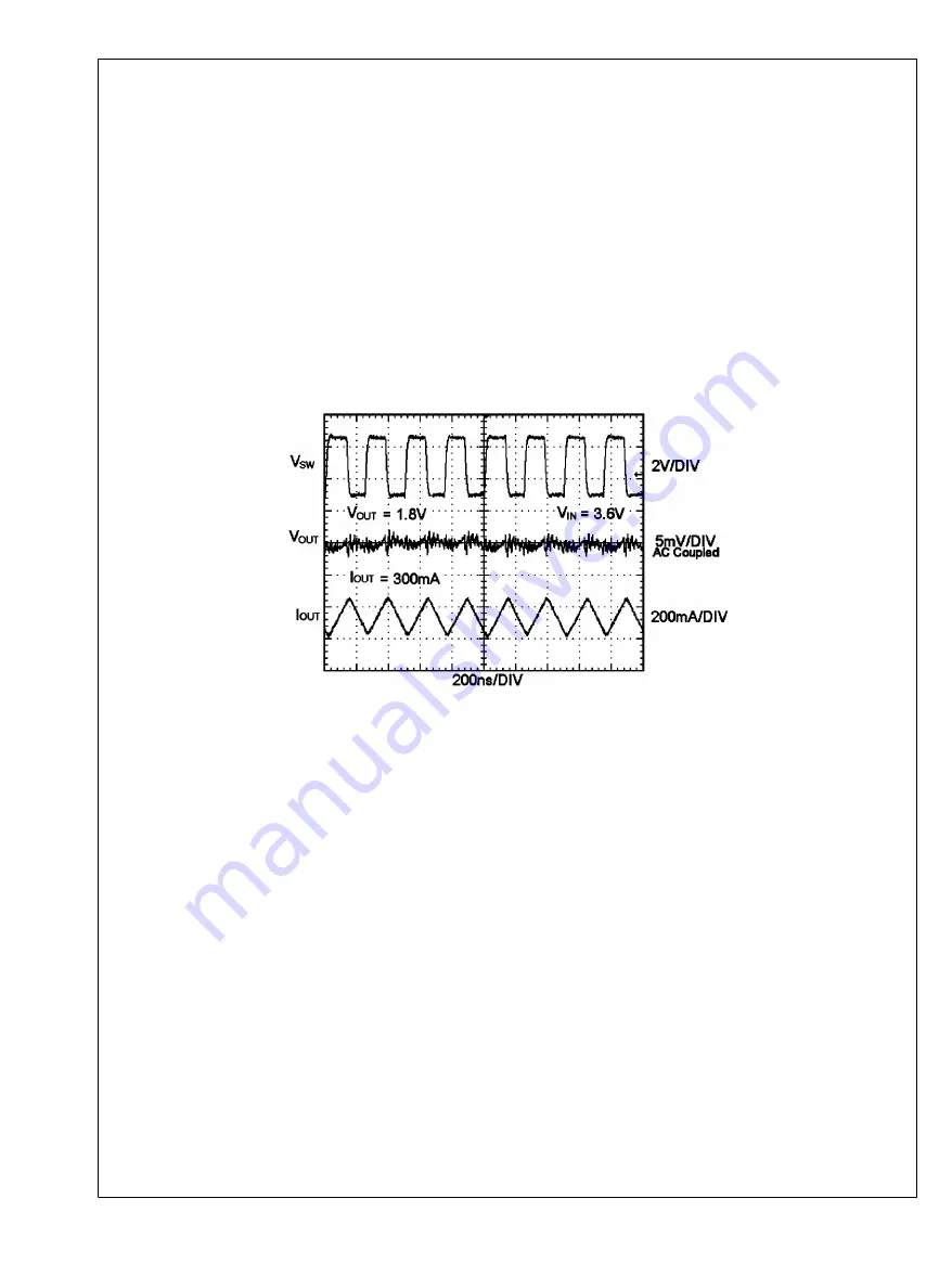
PWM Operation
During PWM operation the converter operates as a voltage-mode controller with input voltage feed forward. This allows the con-
verter to achieve excellent load and line regulation. The DC gain of the power stage is proportional to the input voltage. To eliminate
this dependence, feed forward inversely proportional to the input voltage is introduced. While in PWM mode, the output voltage is
regulated by switching at a constant frequency and then modulating the energy per cycle to control power to the load. At the
beginning of each clock cycle the PMOS switch is turned on and the inductor current ramps up until the comparator trips and the
control logic turns off the switch. The current limit comparator can also turn off the switch in case the current limit of the PMOS is
exceeded. Then the NMOS switch is turned on and the inductor current ramps down. The next cycle is initiated by the clock turning
off the NMOS and turning on the PMOS.
30128232
FIGURE 18. Typical PWM Operation
Internal Synchronous Operation
While in PWM mode, the buck uses an internal NMOS as a synchronous rectifier to reduce rectifier forward voltage drop and
associated power loss. Synchronous rectification provides a significant improvement in efficiency whenever the output voltage is
relatively low compared to the voltage drop across an ordinary rectifier diode.
Current Limiting
A current limit feature allows the device to protect itself and external components during overload conditions. PWM mode imple-
ments current limit using an internal comparator that trips at 1200mA (typ.). If the output is shorted to ground and output voltage
becomes lower than 0.3V (typ.), the device enters a timed current limit mode where the switching frequency will be one fourth, and
NMOS synchronous rectifier is disabled, thereby preventing excess current and thermal runaway.
ECO Mode Operation
The buck switches from ECO state to PWM state based on output load current. At light loads (less than 50mA), the converter
enters ECO mode. In this mode the part operates with low Iq. During ECO operation, the converter positions the output voltage
slightly higher (+30mV typ.) than the nominal output voltage in PWM operation. Because the reference is set higher, the output
voltage increases to reach the target voltage when the part goes from idle state to switching state. Once this voltage is reached
the converter stops switching, thereby reducing switching losses and improving light load efficiency. The output voltage ripple is
slightly higher in ECO mode (30mV peak–peak ripple typ.).
www.ti.com
54
LM49360
Содержание Boomer LM49360
Страница 3: ...5 0 LM49360 Overview 301282h8 FIGURE 1 LM49360 Block Diagram www ti com 2 LM49360...
Страница 4: ...6 0 Typical Application 30128211 FIGURE 2 Sub PMU System Diagram 3 www ti com LM49360...
Страница 5: ...30128216 FIGURE 3 AP PMU System Diagram www ti com 4 LM49360...
Страница 16: ...301282h9 FIGURE 4 PMU State Machine 15 www ti com LM49360...
Страница 68: ...30128213 FIGURE 20 Internal Clock Network 67 www ti com LM49360...
Страница 89: ...301282i1 FIGURE 28 Timing for I2S Master 301282i2 FIGURE 29 Timing for I2S Slave www ti com 88 LM49360...
Страница 128: ...40 0 Schematic Diagram 30128220 FIGURE 36 Demo Board Schematic 127 www ti com LM49360...
Страница 129: ...30128245 FIGURE 37 Demo Board Schematic www ti com 128 LM49360...
Страница 130: ...41 0 Demonstration Board Layout 30128243 FIGURE 38 Top Silkscreen 30128244 FIGURE 39 Top Layer 129 www ti com LM49360...
Страница 131: ...30128238 FIGURE 40 Inner Layer 2 30128239 FIGURE 41 Inner Layer 3 www ti com 130 LM49360...
Страница 132: ...30128240 FIGURE 42 Inner Layer 4 30128241 FIGURE 43 Inner Layer 5 131 www ti com LM49360...
Страница 133: ...30128231 FIGURE 44 Bottom Layer 30128242 FIGURE 45 Bottom Silkscreen www ti com 132 LM49360...
Страница 136: ...Notes 135 www ti com LM49360...


