background image

3 Setup Procedure

This Setup Procedure will detail how to setup the ADC366xEVM hardware and software GUI required for
evaluation using external sample and DCLKIN clocks. The clock rates in the following steps apply specifically to
the ADC3663EVM, but example clock rates are provided for other EVM variants.

3.1 Install High-Speed Data Converter (HSDC) Pro Software

Download the most recent version of the 

HSDC Pro

 software. Launch the executable, and accept the default

installation options.

3.2 Install ADC35XXEVM GUI 1.0 Software

Download the ADC35XXEVM GUI 1.0 software from the EVM tool folder at 

ADC3663EVM

.

Extract and run the executable file, and accept the default installation options.

3.3 Connect the ADC366xEVM and TSW1400EVM

Connect the ADC366xEVM FMC connector to J4 of the LVDS Interposer Card.

Connect J5 of the LVDS Interposer Card to J1 of the TSW1400EVM.

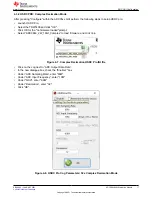
Figure 3-1. ADC366xEVM Complete Setup (external clocks)

Setup Procedure

www.ti.com

6

ADC366xEVM Evaluation Module

SBAU366 – JANUARY 2021

Submit Document Feedback

Copyright © 2021 Texas Instruments Incorporated

Содержание ADC366 EVM Series

Страница 1: ... 1 1 Introduction 2 2 Equipment 2 2 1 ADC366xEVM Functionality 2 2 2 Evaluation Board Feature Identification Summary 4 2 3 Required Equipment 5 3 Setup Procedure 6 3 1 Install High Speed Data Converter HSDC Pro Software 6 3 2 Install ADC35XXEVM GUI 1 0 Software 6 3 3 Connect the ADC366xEVM and TSW1400EVM 6 3 4 Connect the Power Supply and Mini USB Connections 7 3 5 Connect the Clocks and Analog In...

Страница 2: ...tware modifications 2 1 ADC366xEVM Functionality The ADC366xEVM receives power from the USB 2 0 5 V rail and is then converted to 3 3 VDC and 1 8 VDC The ADC receives 1 8 VDC from the TPS62231 DC DC converter The power consumption of the 1 8 V rail can be monitored using the INA226 in the ADC35xxEVM GUI USB to SPI communication is established using the FTDI FT4234H The ADC clocks can be supplied e...

Страница 3: ...EVM block diagram Balun input Figure 2 2 ADC36xxEVM block diagram FDA input www ti com Equipment SBAU366 JANUARY 2021 Submit Document Feedback ADC366xEVM Evaluation Module 3 Copyright 2021 Texas Instruments Incorporated ...

Страница 4: ...e test point labeled 5 EXT The USB data connection is still connected for SPI communications J13 is tied to the REFBUF pin It can be left floating or can be tied to 1 8 V shunt pins 2 3 for normal operation J14 is tied to the PDN SYNC pin It can be left floating for tied to ground shunt pins 1 2 for normal operation To power down the ADC tied to 1 8 V shunt pins 2 3 The ADC may also be powered dow...

Страница 5: ...mmends the following generators Rohde Schwarz SMA100A Rohde Schwarz SMA100B A bandpass filter is required for the analog input signal due to most signal generators addition of phase noise or spurious components A bandpass filter should also be used for the sample clock input The DCLKIN input does not require a bandpass filter If bandpass filters are not used then the true performance of the ADC ma...

Страница 6: ...xecutable and accept the default installation options 3 2 Install ADC35XXEVM GUI 1 0 Software Download the ADC35XXEVM GUI 1 0 software from the EVM tool folder at ADC3663EVM Extract and run the executable file and accept the default installation options 3 3 Connect the ADC366xEVM and TSW1400EVM Connect the ADC366xEVM FMC connector to J4 of the LVDS Interposer Card Connect J5 of the LVDS Interposer...

Страница 7: ...ain the same for all ADC modes For the sample clock ADC3663EVM set a signal generator to 65 MHz at a power level of 10 dBm Connect to the SMA connector J4 A bandpass filter for the sample clock is recommended for best AC performance of the ADC366xEVM For the DCLKIN clock ADC3663EVM set a signal generator to 260 MHz at a power level of 10 dBm A bandpass filter is not required for the DCLKIN clock E...

Страница 8: ...h button switch S1 Also a software reset may be performed at any time to reset the ADC registers to their default state Figure 4 1 ADC35xx Software Reset ADC GUI Configuration www ti com 8 ADC366xEVM Evaluation Module SBAU366 JANUARY 2021 Submit Document Feedback Copyright 2021 Texas Instruments Incorporated ...

Страница 9: ...mple Sample Clock Required DCLKIN Frequency 2 Wire 4 65 MSPS 260 MHz 1 Wire 8 32 MSPS 256 MHz 1 2 Wire 16 10 MSPS 160 MHz For this example ensure that the sampling clock J9 and DCLKIN J7 are connected before launching the ADC35XX EVM GUI In this example for the ADC3663EVM the sampling clock is 65 MHz and the DCLKIN is 292 5 MHz External ADC sampling clock source and DCLKIN source must be frequency...

Страница 10: ...Figure 4 2 ADC35XXEVM GUI ADC3663 Bypass Mode ADC GUI Configuration www ti com 10 ADC366xEVM Evaluation Module SBAU366 JANUARY 2021 Submit Document Feedback Copyright 2021 Texas Instruments Incorporated ...

Страница 11: ...d prompt Select ADC3663_2W_16bit to load firmware and click Yes Enter 65M in the box that says ADC Output Data Rate since the ADC is sampling at 65 MSPS Enter the input frequency of the input signal in the box that says ADC Input Target Frequency 5 MHz used in this example Click Capture www ti com ADC GUI Configuration SBAU366 JANUARY 2021 Submit Document Feedback ADC366xEVM Evaluation Module 11 C...

Страница 12: ...nput signal power may need to be adjusted to reach 1 dBFS ADC GUI Configuration www ti com 12 ADC366xEVM Evaluation Module SBAU366 JANUARY 2021 Submit Document Feedback Copyright 2021 Texas Instruments Incorporated ...

Страница 13: ...Hz signal to J9 sample clock and a 16 25 MHz signal to J7 DCLKIN External ADC sampling clock source and DCLKIN source must be frequency locked If this is not performed the captured data will appear scrambled If using the onboard clocking option the sampling clock and DCLKIN are frequency locked Apply a 1 MHz signal to J2 ensure bandpass filter is used to reduce harmonics and noise of signal genera...

Страница 14: ...663_2W_16bit to load firmware and click Yes Figure 4 4 Real Decimation HSDC Pro INI File 2W 16bit Click on the cog next to ADC Output Data Rate In the new dialogue box enter 65M in ADC Sampling Rate Enter 1M in ADC Input Frequency Enter 16 in Decimation Click OK Click Capture ADC GUI Configuration www ti com 14 ADC366xEVM Evaluation Module SBAU366 JANUARY 2021 Submit Document Feedback Copyright 20...

Страница 15: ...el Real Decimation Figure 4 6 HSDC Pro 16x Real Decimation FFT 2W 16 bit www ti com ADC GUI Configuration SBAU366 JANUARY 2021 Submit Document Feedback ADC366xEVM Evaluation Module 15 Copyright 2021 Texas Instruments Incorporated ...

Страница 16: ...If this is not performed the captured data will appear scrambled If using the onboard clocking option the sampling clock and DCLKIN are frequency locked Apply a 10 MHz signal to J2 ensure bandpass filter is used to reduce harmonics and noise of signal generator An NCO of 9 9 MHz are used to shift the 10 MHz input signal to 100 kHz After launching the ADC35xxEVM GUI perform the following steps Unde...

Страница 17: ...s Figure 4 7 Complex Decimation HSDC Pro INI file Click on the cog next to ADC Output Data Rate In the new dialogue box check the Enable box Under ADC Sampling Rate enter 65M Under ADC Input Frequency enter 10M Under NCO enter 9 9M Under Decimation enter 32 Click OK Figure 4 8 HSDC Pro Cog Parameters 32x Complex Decimation Mode www ti com ADC GUI Configuration SBAU366 JANUARY 2021 Submit Document ...

Страница 18: ...ress Capture Figure 4 9 HSDC Pro 32x Complex Decimation 2W 16 bit ADC GUI Configuration www ti com 18 ADC366xEVM Evaluation Module SBAU366 JANUARY 2021 Submit Document Feedback Copyright 2021 Texas Instruments Incorporated ...

Страница 19: ...clock spurs and broad band phase noise in order to acheive full ADC performance Figure 5 1 ADC3663EVM onboard clocking CDCE6214 65 MHz sample clock 260 MHz DCLKIN The following section shows how to configure and program the ADC366xEVM for onboard clock operation for Real Decimation Mode Onboard clocking can be used for Bypass and Complex Decimation modes as well and uses similar procedures that ha...

Страница 20: ...board Sample Clock Modification DNI R46 R47 Install R41 R51 0 Ω resistor Figure 5 2 ADC36xxEVM Onboard Sample clock modifications Onboard DCLKIN Modification Install R60 and R62 0 Ω resistor DNI R35 and R36 Onboard Clocking Hardware Setup www ti com 20 ADC366xEVM Evaluation Module SBAU366 JANUARY 2021 Submit Document Feedback Copyright 2021 Texas Instruments Incorporated ...

Страница 21: ... 3 ADC36xxEVM Onboard DCLKIN modifications www ti com Onboard Clocking Hardware Setup SBAU366 JANUARY 2021 Submit Document Feedback ADC366xEVM Evaluation Module 21 Copyright 2021 Texas Instruments Incorporated ...

Страница 22: ...tion Configuration The only differences that must be observed in the GUI is the CDC Clock Enable button must be enabled Green and the Configure CDC button must be clicked The PLL_LOCK LED D1 also illuminates to ensure CDCE6214 has been configured correctly Figure 5 4 AD35xx EVM GUI Onboard Clock 16x Real Decimation Onboard Clocking Hardware Setup www ti com 22 ADC366xEVM Evaluation Module SBAU366 ...

Страница 23: ...rocedure shows how to configure the FDA single ended to diferential conversion for CHA The same procedure can be performed for CHB with the respective component designators The edge launched SMA connector J1 receives the single ended analog input signal R1 can be replaced with a capacitor for AC coupling to FDA Modify the following components to complete path to FDA located on top of EVM Install R...

Страница 24: ...components C52 L11 L12 and C53 can be adjusted as the application requires The termination resistors R80 R81 R89 and R90 can be adjusted according to the source impedance Figure 6 3 FDA schematic For further information on the THS4541 FDA please refer to the THS4541 datasheet FDA Configuration www ti com 24 ADC366xEVM Evaluation Module SBAU366 JANUARY 2021 Submit Document Feedback Copyright 2021 T...

Страница 25: ...consumption on the front page of the ADC35XX EVM GUI Click the Measure Power button to refresh the current values This feature is useful for determining what mode sampling speed offers the best power consumption for your application needs Figure 7 1 ADC36xxEVM Power Meter www ti com ADC36xxEVM Power Monitor SBAU366 JANUARY 2021 Submit Document Feedback ADC366xEVM Evaluation Module 25 Copyright 202...

Страница 26: ...red in the Custom Pattern field The digital ramp pattern is now enabled on the ADC The output of the ADC is now an 16 bit incrementing ramp pattern Figure 8 1 ADC36xxEVM 16 bit Ramp Pattern In HSDC Pro the ramp pattern can now be seen when data is captured These same steps apply to any data output mode Bypass Real Decimation and Complex Decimation Trademarks Microsoft and Windows are registered tr...

Страница 27: ...other than TI b the nonconformity resulted from User s design specifications or instructions for such EVMs or improper system design or c User has not paid on time Testing and other quality control techniques are used to the extent TI deems necessary TI does not test all parameters of each EVM User s claims against TI under this Section 2 are void if User fails to notify TI of any apparent defects...

Страница 28: ... These limits are designed to provide reasonable protection against harmful interference in a residential installation This equipment generates uses and can radiate radio frequency energy and if not installed and used in accordance with the instructions may cause harmful interference to radio communications However there is no guarantee that interference will not occur in a particular installation...

Страница 29: ...y for convenience and should be verified by User 1 Use EVMs in a shielded room or any other test facility as defined in the notification 173 issued by Ministry of Internal Affairs and Communications on March 28 2006 based on Sub section 1 1 of Article 6 of the Ministry s Rule for Enforcement of Radio Law of Japan 2 Use EVMs only after User obtains the license of Test Radio Station as provided in R...

Страница 30: ... any interfaces electronic and or mechanical between the EVM and any human body are designed with suitable isolation and means to safely limit accessible leakage currents to minimize the risk of electrical shock hazard User assumes all responsibility and liability for any improper or unsafe handling or use of the EVM by User or its employees affiliates contractors or designees 4 4 User assumes all...

Страница 31: ...OR DAMAGES ARE CLAIMED THE EXISTENCE OF MORE THAN ONE CLAIM SHALL NOT ENLARGE OR EXTEND THIS LIMIT 9 Return Policy Except as otherwise provided TI does not offer any refunds returns or exchanges Furthermore no return of EVM s will be accepted if the package has been opened and no return of the EVM s will be accepted if they are damaged or otherwise not in a resalable condition If User feels it has...

Страница 32: ...s are subject to change without notice TI grants you permission to use these resources only for development of an application that uses the TI products described in the resource Other reproduction and display of these resources is prohibited No license is granted to any other TI intellectual property right or to any third party intellectual property right TI disclaims responsibility for and you wi...

Отзывы: