


TAMC900 User Manual Issue 2.0.1
Page 45 of 71
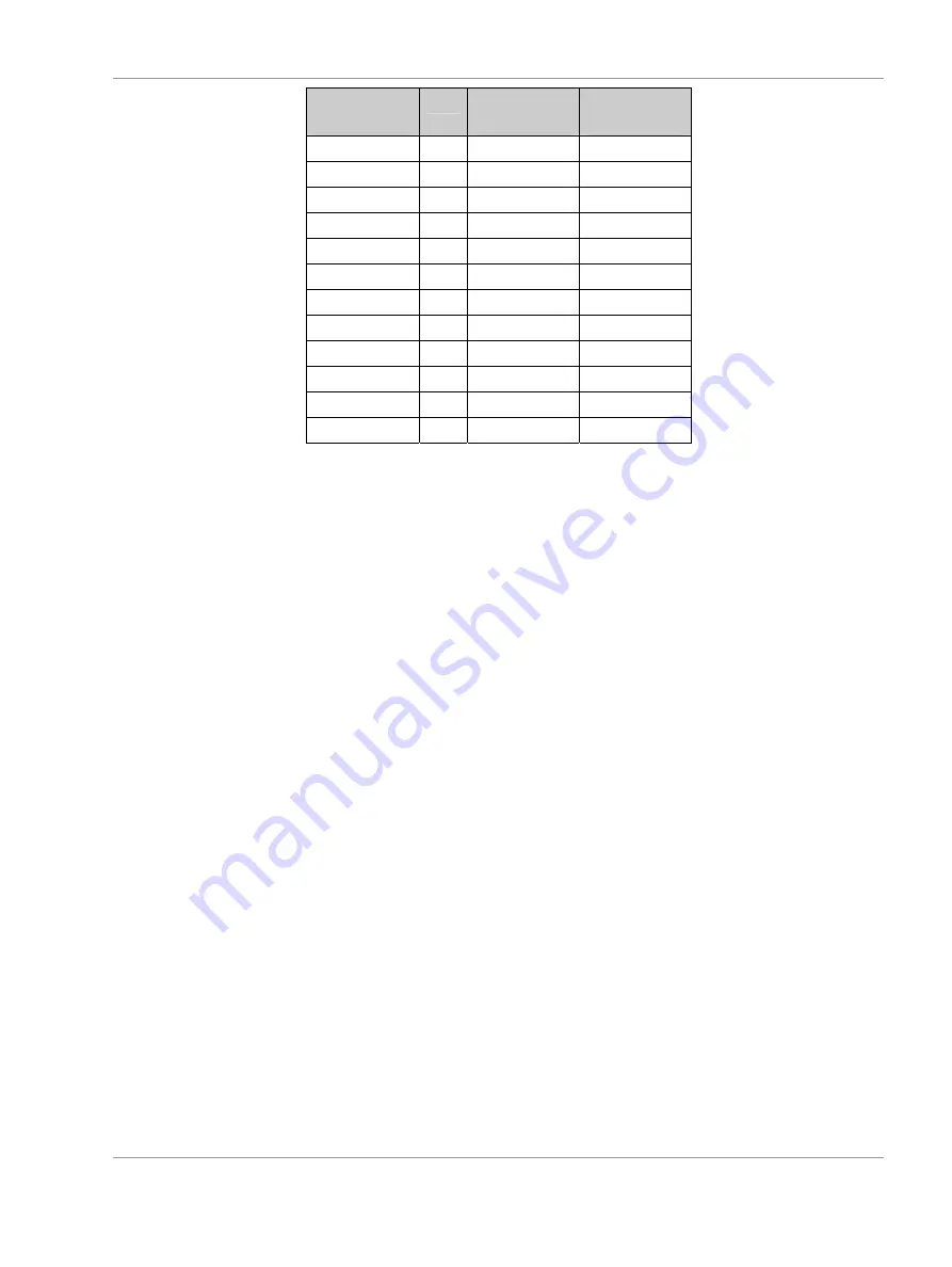
A
IN
+ - A
IN
-
(2V Range)
OF
Data
(Offset Bin.)
Data
(2’s Compl.)
>+1.000000V
1 0x3FFF
0x1FFF
+0.999878V 0 0x3FFF
0x1FFF
+0.999756V 0 0x3FFE
0x1FFE
... ...
... ...
+0.000122V 0 0x2001
0x0001
0.000000V 0 0x2000
0x0000
-0.000122V 0 0x1FFF
0x3FFF
-0.000244V 0 0x1FFE
0x3FFE
... ...
... ...
-0.999878V 0 0x0001
0x2001
-1.000000V 0 0x0000
0x2000
<-1.000000V 1
0x0000
0x2000
Table 9-1 : ADC Output Data Format
The FPGA Logic performs a sign extension of the ADC-Data. Refer to chapter “Channel Logic” for more
information.
9.2.2 Clock Duty Cycle Stabilizer
An optional clock duty cycle stabilizer circuit ensures high performance even if the input clock has a non 50%
duty cycle. Using the clock duty cycle stabilizer is recommended for most applications.
This circuit uses the rising edge of the CLK pin to sample the analog input. The falling edge of CLK is
ignored and the internal falling edge is generated by a phase-locked loop. The input clock duty cycle can
vary from 40% to 60% and the clock duty cycle stabilizer will maintain a constant 50% internal duty cycle.
If the clock is turned off for a long period of time, the duty cycle stabilizer circuit will require a hundred clock
cycles for the PLL to lock onto the input clock.
For applications where the sample rate needs to be changed quickly, the clock duty cycle stabilizer can be
disabled. If the duty cycle stabilizer is disabled, care should be taken to make the sampling clock have a
50% (±5%) duty cycle.