TAMC900 User Manual Issue 2.0.1
Page 10 of 71
1 Product Description
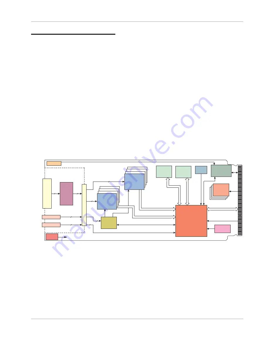
The TAMC900 is a high speed, high performance analog to digital converter AdvancedMC. In addition to the
eight high speed ADCs, it provides excessive preprocessing power by a Virtex-5 FPGA and high speed on
board memory for e.g. full bandwidth snapshots.
The up to x8 PCIe link of the TAMC900 is used to transmit the ADC data to the CPU.
To adapt the TAMC900 to different customer requirements, the TAMC900 is equipped with a Signal
Conditioning Adapter (SiCA) which holds the connector for the analog inputs, the connectors for the clock
and trigger inputs, and the analog signal conditioning.
The TAMC900 provides three clock inputs and three trigger inputs. The three external clock inputs and the
PCIe reference clock are routed to a flexible clocking scheme that allows independent clocking of the ADCs
in two groups. The trigger inputs are routed to the FPGA.
Eight LTC2254 ADCs provide up to 105 MSps and 14 bit resolution each. The minimum sample rate is 1
Msps.
4 MByte high speed on board SRAM enables snapshots of all ADCs at full speed and full resolution for 2ms.
According to AMC.0, the TAMC900 provides an IPMI compliant Module Management Controller (MMC) with
temperature monitoring and hot-swap support.
For First-Time-Buyers the engineering documentation TAMC900-ED is recommended. The engineering
documentation includes TAMC900-DOC, schematics and data sheets of TAMC900.
FPGA
Virtex 5 LX30T
HS-Switch
LEDs
8 x
Diff.
Analog
Input
Config.
Flash
1 x Clock
Signal Conditioning Adapter
(SiCA)
3 x
Trigger
3 x
Clock
8
8
3
3
4
3
3
to MMC
har-link
x8 PCIe
(or User def.)
Trigger
ADC Data
C
lo
ck
2MByte
SRAM
Clock
2MByte
SRAM
Clock
Distribution
4 x ADC
14 Bit
105 MHz
4 x ADC
14 Bit
105 MHz
4
ADC Data
Clock
In
fin
ib
an
d
C
onnec
tor
har-link
Power
Supply
MMC
(IPMI)
S
ignal
C
ond
C
onnect
o
r
A
M
C
-
S
iC
A
Figure 1-1 : Block Diagram TAMC900 with Signal Conditioning Adapter


