


PAGE
3
PC B
OARD
- PC-188 B
ITBUS
I/F
FOR
IBM-PC
O
RDER
NO
. 5904512211
M
AY
2002 - R
EV
. 1.2
1. Bitbus specifications
The Bitbus is a serial communication system based on
electrical code RS485 that employs an SDLC protocol.
The network is based on a hierarchy that has a single
master node that communicates with several slave
nodes. Each slave can work as a master for another
Bitbus network, thereby constituting a multiple hierarchy.
This is particularly useful in applications that require
different transmission rates (Figure 1.1).
Figure 1.1 Typical Bitbus network connection.
The Bitbus interconnection may work in two different
ways: synchronous mode and self-clocked mode. The
first uses a faster transmission rate but is limited as far
as distance and number of network nodes are concerned.
Due to these drawbacks, the PC-188 board uses only
the self-clocked mode.
SELF-CLOCKED MODE:
unlike the previous mode, this
is suitable for long-distance transmission. Two different
transmission rates are employed: 375Kbit/sec and
62.5Kbit/sec. The first transmission rate is able to cover
distances of up to 300m with a max of 28 nodes connected
to the line.
On the other hand, the 62.5Kbit/sec rate covers a max
distance of 1200m with the same number of nodes. For
longer distances, the repeaters have to be used and a
max of 250 nodes can be connected. Figure 1.2 illustrates
the self-clocked mode connection with repeaters.
Figura 1.2 Example of Bitbus network connection in self-
clocked mode with repeaters.
MASTER
MASTER
MASTER
SLAVE
SLAVE
SLAVE
SLAVE
Bitbus
Bitbus
Bitbus
SLAVE
DATA PAIR
DATA PAIR
RTS PAIR
MASTER
SLAVE
SLAVE
REPEATER
REPEATER
REPEATER
Transmission in synchronous mode (not supported) and
self-clocked mode with repeaters is implemented with
screened five-wire cables (a twisted pair for DATA, DATA-
another pair of twisted cables is used for RTS, RTS- and
a RGND reference wire), Figure 1.3.
Figure 1.3 Connections for synchronous or self-clocked mode
with repeaters.
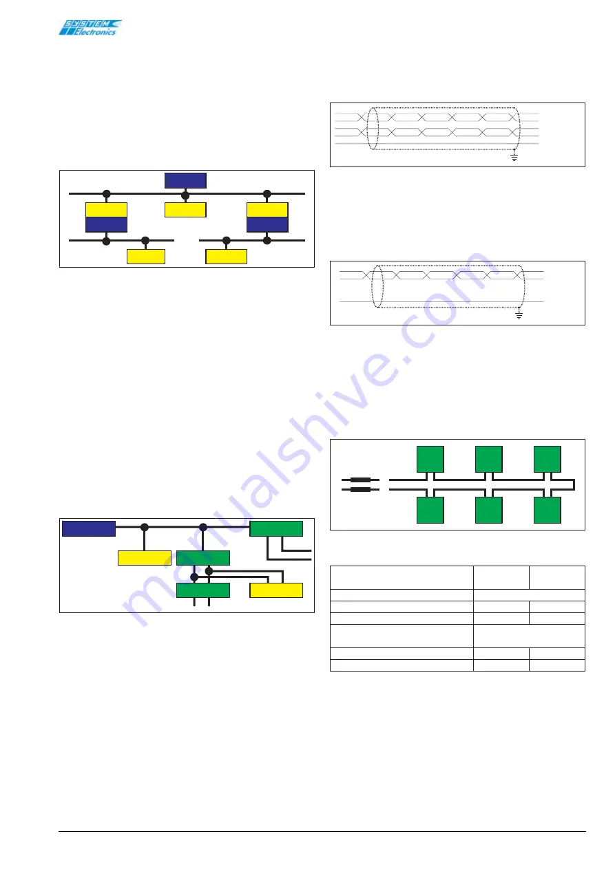
A shielded 3-wire cable is required when using self-
clocked mode without repeaters (a twisted pair dedicated
to DATA and DATA- transmission and a RGND reference
wire), Figure 1.4.
Figura 1.4 Connection for self-clocked without repeaters.
The correct layout of the various modes is shown in
Figure 1.5. In particular, there cannot be any star
networks and, moreover, terminal resistors have to be
placed at either end of the network. The rating of the
terminal resistors has to match the typical impedance
of the connecting cable to prevent reflectance on the
line.
Figure 1.5 Correct layout of Bitbus network nodes.
Table 1.1 Bitbus network operating modes.
DATA
DATA*
DCLK/RTS
DCLK/RTS*
RGND
DATA
DATA*
RGND
R term.
R term.
SELF/CLOCKED
62.5 Kbps
SELF/CLOCKED
375 Kbps
nodes between repeaters
max repeaters on Bitbus line
max nodes on Bitbus line
max distance between repeaters
total distance used by Bitbus line
pairs of lines required
10
251
1200m
13.2Km
1 (no repeaters)
2 (with repeaters)
28
2
84
300m
900m


