6
Hardware layout and configuration
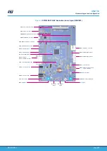
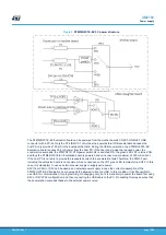
The hardware block diagram (Refer to
) illustrates the connections between the STM32G0C1VET6
microcontroller and the peripherals on the STM32 G0 Evaluation board (such as motor-control connector,
CAN FDs, RS232, RS485, Audio DAC, microphone ADC, TFT LCD, IrDA, IR LED, IR receiver, LDR, microSD
™
card, CEC on two HDMI connectors, Smartcard slot, Temperature sensor).
,
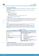
the user to locate these features on the STM32G0C1E-EV Evaluation board.
Figure 3.
Hardware block diagram
Joystick, Key and Tamper button,
LEDs, motor-control connector
GPIOs
USART1
SWD
TIM3_CH1
IR_OUT
IR receiver
IR LED
Voltage
Translator
DB9
connector
USART2
Smartcard
ADC
FDCAN1
CAN-FD
transceiver
STM32G0C1VET6
RS232
transceiver
RS485
transceiver
Embedded
STLINK/
V2-1
Micro-B
USB
connector
USART3
SPI1
Voltage
Translator
MicroSD
TM
card
Dot Matrix
LCD
ADC
DAC
Microphone
Amplifier
Speaker
Amplifier
3.5mm
jack
Potentiometer
2.54 mm
Jumper
FDCAN2
CAN-FD
transceiver
2.54 mm
Jumper
COMP1_INP
I2C2
LDR
HDMI sink
CEC
HDMI source
I2C1
USBC-1
GPIO
USBC-2
Temperature
sensor
I
2
C EXT
connector
DisplayPort
™
sink
MUX
MUX
USB
Type-C
®
connector
USB Power
Delivery
MB1581
mother
board
MB1351 legacy
peripheral
daughterboard
MB1352 USB-C
®
daughterboard
USB
Type-C
®
connector
DisplayPort
™
source
UM2783
Hardware layout and configuration
UM2783
-
Rev 1
page 8/59


