background image

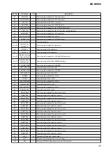
45

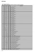
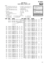
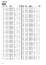
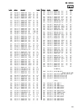
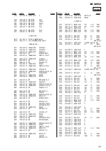
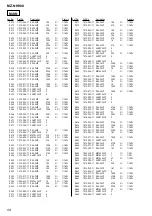
MZ-NH900

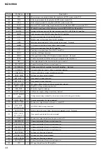
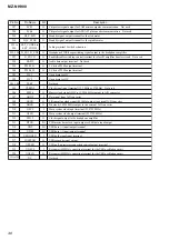
Pin No.

Pin Name

I/O

Description

146

VREFL

I

Reference voltage terminal connected to the capacitor (for the built-in D/A converter L-CH)
Not used

147

AOUTL

O

Built-in D/A converter L-CH signal output    Not used

148

AOUTR

O

Built-in D/A converter R-CH  signal output    Not used

149

VREFR

I

Reference voltage terminal connected to the capacitor (for the built-in D/A converter R-CH) 
Not used

150

DCLSOUTR

O

PWM modulator signal output to the headphone amplifier (R-CH)

151

DCLSOUTL

O

PWM modulator signal output to the headphone amplifier (L-CH)

152

RTCK

Not used

153

ADFG

I

ADIP duplex FM signal (22.05

±

1kHz) input from the RF amplifier

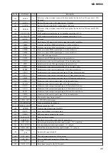
154

TRDR

O

Tracking servo drive PWM signal output (–) to the coil driver

155

TFDR

O

Tracking servo drive PWM signal output (+) to the coil driver

156

FFDR

O

Focus servo drive PWM signal output (+) to the coil driver

157

FRDR

O

Focus servo drive PWM signal output (–) to the coil driver

158

FS4

O

176.4 kHz clock signal output

159

SFDR

O

Sled servo drive PWM signal output to the motor driver

160

SPRD

O

Spindle motor drive control signal output (U) to the motor driver

161

SPFD

O

Spindle servo drive PWM signal output to the motor driver

162

SPDV

O

Spindle motor drive control signal output (V) to the motor driver

163

SPDW

O

Spindle motor drive control signal output (W) to the motor driver

164

SPCU

I

Spindle motor drive comparison signal input (U) from the motor driver

165

SPCV

I

Spindle motor drive comparison signal input (V) from the motor driver

166

SPCW

I

Spindle motor drive comparison signal input (W) from the motor driver

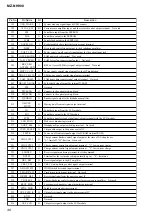
167

SLDV

O

Sled motor drive control signal output (V) to the motor driver

168

SLDW

O

Sled motor drive control signal output (W) to the motor driver

169

SLCU

I

Sled motor drive comparison signal input (U) from the motor driver

170

SLCV

I

Sled motor drive comparison signal input (V) from the motor driver

171

SLCW

I

Sled motor drive comparison signal input (W) from the motor driver

172

SRDR

O

Sled motor drive control signal output (U) to the motor driver

173

DIN

I

Digital audio signal input terminal

174

FS256_OUT

O

11.2896 MHz clock output

175

CHOPPERCLK

O

Clock signal output for chopper

176 to 179

MNT0 to MNT3

O

Monitor output for DSP

180

OFTRK

I/O

Tracking signal input/output for MD3

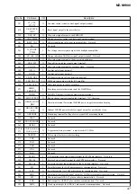
181

RECP

O

Laser power changeover signal output

182

EFMO

O

EFM encode data output for the record

183

PAUSE_KEY

I

Pause key input terminal

184

PROTECT

I

Recording protector detection input for normal disc

185

OPT_DET

I

Optical digital input plug detection input terminal    “H”: optical in

186

XJACK_DET

I

Line input plug detection input terminal    “L”: plug in

187

XMIC_DET

I

Microphone input plug detection input terminal    “L”: plug in

188

OPEN_CLOSE

_SW

I

Open switch input terminal

189

XCS_ADC

O

Chip select signal output for A/D converter

190

XPD_ADC

O

Power control signal output for A/D converter

191

 NC

Not used

192

XRST_LCD

O

Reset signal output for the LCD module

Содержание Walkman MZ-MH900

Страница 1: ... LR6 size AA alkaline battery Battery charging stand AC power adaptor DC 3V Operating temperature 5 C 41 F to 35 C 95 F Dimensions Approx 81 3 77 8 21 2 mm w h d 31 4 31 8 27 32 in excluding projecting parts and controls Mass Approx 110 g 3 9 oz the recorder only Approx 133 g 4 7 oz including the Supplied accessories AC power adaptor 1 Battery charging stand 1 Remote control 1 Headphones for USA m...

Страница 2: ...ording continuously in MD mode Unit approx hours JEITA When playing continuously in Hi MD mode Unit approx hours JEITA When playing continuously in MD mode Unit approx hours JEITA Battery life When recording continuously in Hi MD mode Unit approx hours JEITA1 Disc type Batteries Linear PCM Hi SP Hi LP 1GB Hi MD disc NH 10WM2 3 5 5 6 LR63 2 5 3 5 4 NH 10WM LR6 6 8 5 10 60 74 80 minute standard disc...

Страница 3: ...on 23 6 2 Block Diagram AUDIO Section 24 6 3 Block Diagram POWER SUPPLY Section 25 6 4 Schematic Diagram MAIN Section 1 9 27 6 5 Schematic Diagram MAIN Section 2 9 28 6 6 Schematic Diagram MAIN Section 3 9 29 6 7 Schematic Diagram MAIN Section 4 9 30 6 8 Schematic Diagram MAIN Section 5 9 31 6 9 Schematic Diagram MAIN Section 6 9 32 6 10 Schematic Diagram MAIN Section 7 9 33 6 11 Schematic Diagram...

Страница 4: ...e viscou s sticky less prone to flow than ordinary solder so use caution not to let solder bridges occur such as on IC pins etc Usable with ordinary solder It is best to use only unleaded solder but unleaded solder may also be added to ordinary solder Providing the required system environment The following system environment is required in order to use the SonicStage MD Simple Burner software for ...

Страница 5: ...e direction of the arrow to disable the buttons on the recorder To prevent the buttons from being accidentally operated when you carry the recorder use this function S i headphones earphones LINE OUT jack Looking at controls The display window of the recorder A Character information display Displays the disc and track names date error messages track numbers etc B SYNC synchro recording indication ...

Страница 6: ...ng of the previous track rewind Press towards find the beginning of the next track fast forward 1 2 Using the clip for the remote control It may be hard for you to read the indications in the display if the remote control is attached upside down with the clip in its current position In this case attach the clip in the opposite direction as shown below 1 Remove the clip 2 Attach the clip in the opp...

Страница 7: ...ge 9 3 7 GEAR BSA GEAR SB Page 10 3 8 OP SERVICE ASSY Page 11 3 9 DC MOTOR SSM18D C NP SPINDLE M701 DC MOTOR SLED M702 DC MOTOR UNIT OVER WRITE HEAD UP DOWN M703 Page 11 3 10 HOLDER ASSY Page 12 3 6 BATTERY CASE BLOCK Page 10 SET Note 1 The process described in can be performed in any order Note 2 Without completing the process described in the next process can not be performed SECTION 3 DISASSEMB...

Страница 8: ... battery lid in the direction of arrow 2 battery lid 3 screw M1 4 4 two screws M1 4 6 case lower block 5 two screws M1 4 7 three toothed lock screws M1 4 6 two toothed lock screws M1 4 4 flexible board CN701 0 MAIN board 8 5 flexible board CN471 9 flexible board CN501 2 flexible board 1 Remove two solders 3 Remove the solder ...

Страница 9: ...NH900 181 B A 4 two screws M1 4 3 two screws M1 4 5 upper panel block 1 flexible board CN471 2 Slide the open slider in the direction of arrow A and open the upper panel sub assy in the direction of arrow B 2 mechanism deck MT MZNH900 181 1 two step screws MD ...

Страница 10: ...GEAR SB 1 self tap screw 2 thrust retainer spring 3 washer 0 8 2 5 4 gear BSA 5 gear SB 3 6 BATTERY CASE BLOCK 4 screw M1 4 7 battery case block 5 tension spring lock 6 open slider 2 MD standard pin 1 claw 3 two screws 1 7 2 5 ...

Страница 11: ... screw block assy is turned and it removes from OP service assy 2 OP service assy 3 two screws M1 4 4 DC motor sled M702 1 Remove four solders of flexible board 2 Remove two solders of flexible board 6 three self tap screws 7 DC motor SSM18D C NP spindle M701 5 motor base assy 9 DC motor unit over write head up down M703 8 self tap screw ...

Страница 12: ...lled once A cable is not rolled A cable is rolled once clamp filter ferrite core Part No 1 543 793 41 clamp filter ferrite core Part No 1 543 793 41 clamp filter ferrite core Part No 1 543 793 41 clamp filter ferrite core Part No 1 543 793 41 clamp filter ferrite core Part No 1 543 798 31 clamp filter ferrite core Part No 1 543 798 31 clamp filter ferrite core Part No 1 543 798 31 A cable is rolle...

Страница 13: ... version number Note Once the test mode is activated with this application the test mode is then activated forcibly by only turning on the power After the repair completed be sure to release the test mode by using this application once more 2 OPERATION IN SETTING THE TEST MODE When the test mode becomes active first the Display Check mode is selected Other mode can be selected from the Display Che...

Страница 14: ...000th place of item number increase VOL key 1000th place of item number decrease VOL key 100th place of item number increase VOL key 100th place of item number decrease Medium item switching x key key VOL key 10th place of item number increase VOL key 10th place of item number decrease Minor item switching key 1st place of item number increase key 1st place of item number decrease VOL key Increase...

Страница 15: ...not setting the temperature correction value NotCD Does not complete the CD Overall adjustment beforethe MD1 Overall adjustment NotM1 Does not complete the MD1 Overall adjustment before the Hi MD3 Overall adjustment NotH3 Does not complete the Hi MD3 Overall adjustment before the Stray Light Offset Overall adjustment NG Error of item number 7 SELF DIAGNOSIS RESULT DISPLAY MODE This set uses the se...

Страница 16: ...ear the total recording time 8 KEY CHECK MODE This mode is used for key check Operation of The Key Check Mode 1 Enter the test mode Display Check mode 2 Press the GROUP key to activate the Key Check mode where the LCD displays as shown below Display Remote commander 0 with 4 without Pressed key name When remote commander key is pressed display becomes as r When the jog dial is turned it displays J...

Страница 17: ...ction check 6 Laser power check 7 Setting the adjustment values 8 Servo Overall adjustment 9 Resume clear 10 Releasing the test mode 3 ADJUSTMENT OF THE EACH ITEM 3 1 Entering The Test Mode Refer to the SECTION 4 TEST MODE 3 2 Initialize The Adjustment Value Procedure 1 In the test mode Display Check mode press the VOL key to enter the Overall adjustment mode 2 Press the T MARK key and display 911...

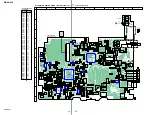
Страница 18: ...R526 Q884 2E 2B 1C 2C 1B 1E Q881 1E 1B 2C 1C 2B 2E D882 D883 A K A K D884 K A L881 L801 C805 C818 R869 C859 FB808 C838 L804 IC801 C883 Q504 B C E C567 L506 SL802 SL901 IC501 5451 48 45 43 42 40 37 34 31 5552 49 47 44 41 38 36 33 30 5653 50 46 39 35 32 29 1 4 7 11 18 22 25 28 2 5 8 10 13 16 19 21 24 27 3 6 9 12 14 15 17 20 23 26 C553 C518 C556 C564 L503 L505 L507 Q503 B C E Q502 B C E C570 D885 D90...

Страница 19: ...L key to enter the Manual mode 4 Press the VOL key twice to display as follows Display 5 Press the key once press the VOL key once press the key once press the VOL key three times and press the key once to display as follows Display 6 Adjust with VOL VOL keys so that the value of digital voltmeter becomes 1 80 V 7 Press the X key to write the adjusted value 8 Press the key to select the next item ...

Страница 20: ... VOL key to enter the Manual mode 2 Open the lid and press the key continuously until the optical pick up moves to the most inward track 3 Set the laser power meter so that the laser beam from the optical pick up aims at the objective lens of laser power meter at right angle 4 Press the VOL key once to display as follows Display 5 Press the key three times to select the item number 9111 and displa...

Страница 21: ...d on the LCD 9 Insert the Hi MD3 adjustment disc HMD1GSDJ 10 Put the main unit horizontal so that the LCD becomes upside and press the VOL key 11 Wait until HMD OK is displayed on the LCD 12 Eject the disc 13 Put the main unit horizontal so that the LCD becomes upside and press the VOL key 14 Wait until OfstOK is displayed on the LCD 15 Press the x key and back to the Display Check mode 3 9 Resume...

Страница 22: ...22 MZ NH900 MEMO ...
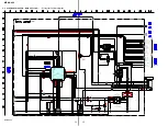
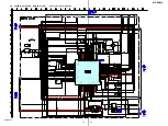
Страница 23: ...3 180 VREF_MON OFTRK APCREF_DA SYSTEM CONTROLLER DIGITAL SIGNAL PROCESSOR IC801 1 3 A CLK SLCU SLCV SPCU SPCV SPCW SLD MON U SLD MON V CLV MON U CLV MON V CLV MON W SPRD SPDL_MON SLDW SLDV SRDR SLD_MON FRDR FFDR TRDR TFDR SPDV SPDW XRST_MTR_DRV RI1 FI1 RI2 FI2 WI2 VI2 UI2 VI1 WI1 CPWO2 CPVO2 CPUO2 SLD MON W SLD MON V SLD MON U STALL UI1 PWM1 FO2 FCS FCS TRK TRK COM2 WO1 CPVI2 WO2 CPUI2 CPWI2 CPUI1...

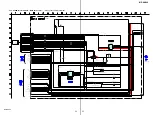
Страница 24: ...G_A 249 JOG_B 227 XHOLD_SW 183 PAUSE_KEY 124 SET_KEY_1 125 SET_KEY_2 213 SI1 214 SO1 215 SCK1 236 XCS_LCD 192 XRST_LCD RESET SWITCH Q471 T_MARK JOG_A JOG_B HOLD PAUSE SET_KEY_1 SET_KEY_2 SDI SDO SCK CS LCD MODULE RST XWK DVDD XWK1 XWK4 DDC3 B REG VSTB B 2 4V REGULATOR IC471 253 S891 Hi MD PROTECT DETECT HIMD_PROTECT 188 S893 OPEN CLOSE DETECT OPEN_CLOSE_SW 184 S890 PROTECT DETECT PROTECT 135 S892 ...

Страница 25: ... SCK 54 VBUS 36 VPDRV 88 PVBUS 43 VBUSSEL 38 CLP 42 CLM 37 POWP1 41 POWP2 91 DVDD_OUT REG5 B 3 2V REGULATOR IC603 2 1V REGULATOR IC882 DC DC CONVERTER IC881 98 REG_OUT 1 2V REGULATOR IC602 REG5 OSC B REG F B 93 OSC_OUT 2 5V REGULATOR IC804 USB IF VDD 108 V33RO 13 VC VC B D609 61 VIF 14 VC 67 RECP 250 VBUS_DET 51 VBUS_DET 316 USBHOLD 86 HOLD_OUT 317 SUSPEND 99 SUS_IN 132 RST_CONT 95 RST_IN REG5 VST...

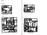
Страница 26: ...ion EE East European model Note on Printed Wiring Board X parts extracted from the component side Y parts extracted from the conductor side f internal component Pattern from the side which enables seeing The other layers patterns are not indicated Caution Pattern face side Parts on the pattern face side seen from Conductor Side the pattern face are indicated Parts face side Parts on the parts face...

Страница 27: ...LD_CON_U SLD_PWM SLD_MON_U SLD_MON_V SLD_MON_W CLV_CON_U CLV_CON_V CLV_PWM CLV_MON_U CLV_MON_V CLV_MON_W CLV_CON_W CLV_CON_W CLV_CON_V CLV_CON_U CLV_PWM CLV_MON_U CLV_MON_V CLV_MON_W FF1 TF1 TR1 FR1 FF1 FR1 TF1 TR1 ZI1 ZI2 ZI1 ZI2 HD_DRV HD_DRV CLVW CLVV CLVU CLVN SLEDN SLEDU SLEDV SLEDW VI2 UI2 PWM2 CPUO2 CPVO2 CPWO2 STALL GND VCC VG CPWO1 CPVO1 CPUO1 PWM1 UI1 VI1 WI1 PGNDW1 WO1 ST1 VMVW1 VO1 VO1...

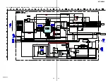
Страница 28: ... 0 10 6 3V 0 0 0 0 MCH6617 TL E 33p 100V MA2Z748001S0 220 A1 A2 A3 A4 A5 C1 C2 C3 E1 E2 E3 E4 E5 E6 E7 E8 E9 E10 E11 E13 F1 D1 D2 F2 VB RMC_DTCK VBUS_VB_CTL XCS_REC_DRV VBUS_DET DDC3 REG_F EFM_CLK EFM RECP SUSPEND USB_HOLD 3 3V 4FS SDO0 SCK0 RST_CONT SLEEP VREC_SEL XRST REG5_REG REG5_VSTB REG5_OSC REG4_DVDD REG_DACVREFH TERRA_V RADIO_ON VREC_SEL XCS_REC_DRV XCS_REC_DRV VBUS_DET VBUS_DET REG_F REG_...

Страница 29: ...C4738F Y GR TPL3 47k L505 10µH 10k 47k 0 1 4 7 6 3V 4700p 0 10k 47k 0 0 1 1k 4700p 0 220 470 100p 0 1 4 7 6 3V 1 2 2k 1k 0 1 0 1 0 1 0 1 26P 1 0 01 0 1 0 0 2SC4627J C TX SO MCH6604 SN761059ZQLR R1180Q301B 0 1 10 1 4 7 6 3V B1 B2 B3 C1 C2 C3 I1 I2 REG03 LC_DRV1 LC_DRV2 PEAK PLSE_XDC XLDON BOTM OFTRK MDVCC_CTL RFI VIN ADIP VC S_MON APCREF_DA SSB_DATA SSB_CLK XRST_RF VREF ABCD FE TE A_FS256 S1 S0 LC_...

Страница 30: ...B TP 1 BATT BATT 220 5V VBUS 5V 2200p 0 VBUS GND GND 0 01 0 0 1 3P 0 1 0 1 0 1 MA22D2800LS0 SI1410EDH T1 MA22D2800LS0 100k 10k 4 7k 1M 0 1 02DZ2 4 Z THP3 MAZS068008SO 0 1 220 5V 0 1 D1 G1 G2 G3 H1 D2 M1 G4 M3 M2 UDP UDM GND_SW VBUS_MON MINUS_MON TERRA_V CHG_MON CHG_I_CTL2 CHG_I_CTL3 CHG_PWM HIDC_MON CHG_TYPE2 STAND_DET NI_VI_CTL UDM UDP CHG_PWM CHG_I_CTL2 CHG_I_CTL3 CHG_MON CHG_TYPE2 CHG_PWM UDP U...

Страница 31: ...000p 10k 100p 1000p 220k 470k 470k 0 2 2 0 01 220k 22k 100k 1000p 2 2 22k 47k 100p MA22D2800LS0 0 1 TS8K1TB 47k 22 6 3V 22 6 3V 2 2 22 6 3V 0 1 22k 22k 1k 47k 100k 0 01 XC61CC1702NR 0 100k 0 1 XC62HR5502MR 2 2 2 2 100k 47k 100k 220k 1 100 L907 47µH L904 10µH 4 7 0 0 0 470k 2 2k 470k XP4601 TXE 47k E1 E2 E3 E4 E5 E6 E7 E8 E9 E10 E11 E13 G1 G2 G3 I1 I2 J1 J2 J4 J5 L1 L2 G4 J7 J8 J9 J6 SDO0 SCK0 4FS ...

Страница 32: ...P4314 TX SI1410EDH T1 220 2 5V 220 Q1 H1 F1 F2 J9 J8 J7 J5 J1 J4 J2 J6 BEEP RMC_KEY XCS_PWR_IC WK_DET REC_KEY HALF_LOCK D_VREG0 D_VCONT_PWM DCLSOUTR DCLSOUTL D_ENVG D_ENREG D_EN2 D_EN1 FS512 XMUTE GND S_GND XRST2 BEEP RMC_DTCK RMC_KEY RMC_KEY XCS_PWR_IC WK_DET REC_KEY HALF_LOCK XMUTE FS512 D_EN1 D_EN2 D_ENREG BEEP DCLSOUTL DCLSOUTR D_VCONT_PWM D_VREG0 D_VCONT_PWM DCLSOUTR DCLSOUTL D_ENVG D_ENREG D...

Страница 33: ...REG5_OSC REG4_DVDD XCS_PWR_IC WK_DET REC_KEY HALF_LOCK XRST2 S_GND GND REG_DACVREFM RADIO_ON REG5_REG REG5_VSTB SDI0 XCS_NV SDO0 SCK0 WK_DET REC_KEY HALF_LOCK XRST2 RMC_KEY XCS_PWR_IC XCS_LCD SDI1 SDO1 SCK1 LCD_RST JOG_B JOG_A SET_KEY_2 SET_KEY_1 REC_KEY WK_DET XHOLD_SW PAUSE XRST2 RMC_DTCK 4FS SDO0 SCK0 RST_CONT SLEEP VREC_SEL XRST REG_F REG5_REG 3 3V REG5_VSTB REG5_OSC REG4_DVDD HIMD_PROTECT PRO...

Страница 34: ...I2 ZI1 REG_DACVREFM XLDON GND_SW VBUS_MON MINUS_MON XRST_MTR_DRV RECP SCK1 SDO1 CHG_MON CHG_MON CHG_I_CTL2 CHG_I_CTL3 CHG_I_CTL2 CHG_I_CTL3 CHG_PWM CHG_PWM HIDC_MON HIDC_MON CHG_TYPE2 CHG_TYPE2 SCK0 SDO0 XBCK LRCK FS256 XCS_ADC ADDT DIN1 XJACK_DET OPT_DET RMC_DTCK XOPT_CTL XOPT_CTL XPD_ADC XPD_ADC XCS_ADC XJACK_DET OPT_DET DIN1 S0 S1 FS256 ADDT LRCK XBCK S1 S0 DRAM_HOLD_DET DRAM_VDD_CLR DRAM_ALONE...

Страница 35: ...1 10k 1 1M 100k MA2Z748001S0 MA2SD32008S0 MA2SD32008S0 XP4314 TX 47k 220k 2 2M 220k 10k 0 1 MAZS068008SO MAZS068008SO MAZS068008SO SI1410EDH T1 R1180Q221B 0 XP4314 TX MA2Z748001S0 470k 100 0 0 MAZS068008SO 4 7 6 3V 4 7 6 3V 47 4V 47 4V AK5356VN L 2 2 6 3V 10 6 3V 47 6 3V 0 1 0 1 10 6 3V 22 6 3V 10k 22k 0 1 1000p 1000p 2200p 2200p 22k 10k 0 1 1 1 100 100 0 0 0 0 1 0 1 0 1 0 1 0 L1 M2 M1 P3 P4 L2 M3...

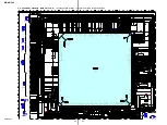
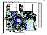
Страница 36: ...A D904 A K D801 Q801 A K R642 R641 R801 R865 R837 C827 C835 C902 C892 C853 C828 R857 R856 R894 R833 C926 R895 R866 R897 C960 C901 C434 R923 R442 R939 R443 C961 C959 R444 C903 R903 R906 R931 R924 R967 R950 R940 R968 R938 R937 R969 L805 L903 L904 L702 L501 L701 C915 C918 C931 C933 C812 C864 FB807 L806 C808 C885 C887 FB803 FB802 FB809 C935 C936 C942 C937 C941 C919 C906 Q904 S D D G D D C916 Q905 1E 1...

Страница 37: ...R353 R645 R434 R414 R415 R652 Q407 B C E D602 A K D603 A K L601 L603 C672 L907 C627 C658 C315 C362 C316 C323 C108 C107 C321 C635 Q901 5 8 4 1 L605 SL891 SL892 SL701 L504 L502 S894 C637 C621 C607 C609 C619 C367 C354 C365 C360 C351 R608 C368 FB471 R362 C364 C370 C601 C613 IC601 IC605 57 56 54 52 49 45 41 37 34 32 30 29 58 59 55 53 50 46 42 38 35 33 31 28 84 87 89 91 94 98 102106 109 111 3 2 85 86 88...

Страница 38: ... JX JY LY OFTRK TON C AVCC2 VCC2 TEMP VREF09 A C D C MALFA MIJ AWBPF DW DWBPF OFTTH APC ADIP BPF VFREF0 4 I J A B C D I J NPP TON CSL AW DW TON PEAK TON BOTM ADIP TE TWPP PK BTM AW CSLO S MONITOR VREF A D CONVERTER A D VREF VREF A7CAL_SW 13 WDT 10 LED_CTL 9 IAMP_CTL 14 CFB 15 TYPE1 11 BAT 31 CHG_SW1 30 I_CTL2 29 BAT 25 RF1 26 IAMP_CAL 27 AMP_SEL 28 VO 32 22 I_CTL3 23 RS 24 I_CTL1 20 I_SEL 18 AD_SE...

Страница 39: ...3 67 RECP 68 GND 69 HBB 70 HAB 71 CH 72 GND 73 VG2 74 VCP 75 CL 76 PGND4 77 HB 78 HA 79 PGND2 80 VRECIN 81 VRECIN 82 OUTB 83 VG 84 OUTA 89 CRST 90 DVDD IN 91 DVDD OUT 92 HOLDC 93 OSC OUT 94 SLEEP IN 95 RST IN 96 PGND2 97 REG IN 98 REG OUT 99 SUS IN 100 PGND2 101 TSBV IN 102 TSBV OUT 103 V33R 104 PGND1 105 VSTB IN 106 VSTB OUT 107 BATSEL 108 V33RO 109 RF1 110 INM1 111 DTC1 112 VREC HOLD LOGIC BUFFE...

Страница 40: ... 11 VMU1 VI1 49 VI2 63 UI1 50 UI2 62 PWM1 61 CPUO1 60 CPVO1 59 CPWO1 51 PWM2 52 CPUO2 53 CPVO2 54 CPWO2 STANDBY 55 STALL 56 GND 57 VCC 58 VG DECODER 7 VO1 6 VO1 10 UO1 9 UO1 12 VMR1 15 PGND1 14 RO1 13 RO1 16 FO1 32 FO2 19 FI1 20 RI1 29 RI2 30 FI2 21 COM1 22 CPUI1 23 CPVI1 VG PRE DRIVE VG VG VG PRE DRIVE VG PRE DRIVE 24 CPWI1 25 CPWI2 26 CPVI2 27 CPUI2 28 COM2 33 FO2 34 PGND2 37 VMR2 38 VMU2 39 UO2...

Страница 41: ...T2 20 DTC1 19 XRST1ADJ 18 CRST1 17 XRST1 25 LG 24 VG 26 PGND3 23 C1L 29 VGSEL1 28 VGSEL2 30 INM2 31 RF2 32 DTC2 RST2 REF2 VG SELECT VG DUTY CLK 36 PGND2 35 PGND2 L2 37 L2 38 VO2 39 VCO2 40 VCIN 41 VC2 42 DW 2T 43 DW 2B 44 MUTEON 45 REGC3 46 REGO3 47 REGI3 48 SERIAL PASS REGULATOR 2 SERIAL PASS REGULATOR 1 RST1 RST2 SEQSEL MUTE ON MUTING BUFFER VC2 RST2 POWER SWITCH 1 RST2 STEP UP DOWN DRIVER PWM S...

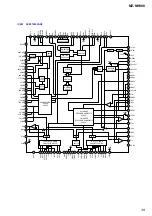
Страница 42: ... DVDD1_10 Power supply terminal 24 DVSS1_10 Ground terminal 25 DVDD1_11 Power supply terminal 26 DVSS1_11 Ground terminal 27 AVDD1A Power supply terminal for PLL 28 AVSS1A Ground terminal for PLL 29 AVDD1B Power supply terminal 30 AVSS1B Ground terminal 31 AVDD1C Power supply terminal 32 AVDD2 Power supply terminal for A D converter 33 DVDD25SVADC Power supply terminal for A D converter 34 AVSS2 G...

Страница 43: ... supply terminal for AUX 78 FVSS0 Ground terminal for AUX 79 SRAMVDD0 Power supply terminal for AUX 80 SRAMVSS0 Ground terminal for AUX 81 SRAMVDD1 Power supply terminal for AUX 82 SRAMVSS1 Ground terminal for AUX 83 EBIFVDD0 Power supply terminal for interface circuit 84 EBIFVSS0 Ground terminal for interface circuit 85 EBIFVDD1 Power supply terminal for interface circuit 86 EBIFVSS1 Ground termi...

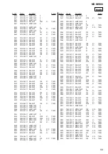
Страница 44: ...y of regulator for class D amplifier Not used 121 VB_MON I Unregulated power supply voltage monitoring terminal 122 CHG_MON I Charge or discharge current monitoring terminal 123 VREF_MON O Reference voltage output terminal 124 SET_KEY_1 I Front panel key input terminal 125 SET_KEY_2 I Front panel key input terminal 126 STAND_DET I DC input voltage for battery charge monitoring terminal 127 HIDC_MO...

Страница 45: ...arison signal input U from the motor driver 165 SPCV I Spindle motor drive comparison signal input V from the motor driver 166 SPCW I Spindle motor drive comparison signal input W from the motor driver 167 SLDV O Sled motor drive control signal output V to the motor driver 168 SLDW O Sled motor drive control signal output W to the motor driver 169 SLCU I Sled motor drive comparison signal input U ...

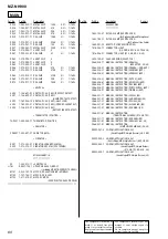
Страница 46: ...input from the LCD module 214 SO1 O Serial data output to the LCD module 215 SCK1 I O Serial data transfer clock signal input output terminal with the LCD module 216 SLD_MON I Sled servo monitoring terminal 217 AOUT_SEL O Headphone line output switching terminal Not used 218 YUZU_SLEEP O Chip enable output to the power control IC 219 FFCLR O Power on off control signal output for FCRAM internal RA...

Страница 47: ...minal 255 CHG_TYPE2 O Battery charge control signal output terminal H charging 256 DRAM_HOLD _DET I Detection terminal for internal D RAM power supply information keeping 257 DRAM_VDD _CLR O Internal D RAM power latch clear signal output for quick mode sleep 258 AD2ENDF I Monitoring terminal for flag of servo signal A D measuring finish 259 TEST Not used 260 SRAM_MODE I Not used 261 HSALF I Not us...

Страница 48: ...TEST Not used 305 CLKIN2 I Clock signal input terminal 13 5 MHz or 27 MHz Not used 306 FS256 O Master clock signal 256Fs 11 2896 MHz output to A D converter 307 ADDT I Data input from A D converter 308 LRCK O L R sampling clock signal 44 1kHz output to external A D converter 309 XBCK O Bit clock 2 8224 MHz output to the external A D converter 310 OSCI I Main system clock input terminal 22 5792 MHz...

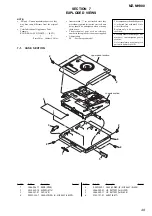
Страница 49: ... EE East European model NOTE XX and X mean standardized parts so they may have some difference from the original one Color Indication of Appearance Parts Example KNOB BALANCE WHITE RED Parts Color Cabinet s Color 1 2 2 2 2 2 3 6 4 5 upper panel section chassis section 4 X 2023 389 1 CASE LOWER B SUB ASSY BLACK 5 3 266 509 01 LID BATTERY for SILVER 5 3 266 509 11 LID BATTERY for BLACK 6 2 188 727 0...

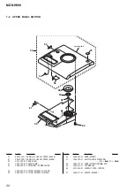
Страница 50: ...KNOB HOLD 53 3 264 154 01 BADGE HI MD 54 3 266 488 01 SPRING REC COMPRESSION 55 3 266 485 01 BUTTON T MARK for SILVER 55 3 266 485 11 BUTTON T MARK for BLACK 56 3 266 492 01 KNOB ROTARY 57 3 266 192 01 ESCUTCHEON 5 DIRECTION VOL VOL 58 3 266 191 01 KNOB 5 DIRECTION N ENT 59 1 805 513 11 LCD MODULE 60 3 318 382 91 SCREW 1 7X2 5 TAPPING 61 3 266 577 01 SPACER HOLDER 51 52 53 54 55 56 57 61 58 59 60 ...

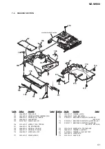
Страница 51: ...1 SPRING R TORSION 110 3 246 996 01 SCREW MD STEP 111 3 242 558 01 SPACER LINE IN 112 3 245 901 01 TERMINAL SUM 3 113 3 245 902 01 COVER INSULATING 114 X 2023 375 1 MAIN BOARD COMPLETE for SERVICE AEP UK EE 114 X 2023 376 1 MAIN BOARD COMPLETE for SERVICE US 114 X 2023 377 1 MAIN BOARD COMPLETE for SERVICE EXCEPT US AEP UK EE 115 3 238 876 04 SCREW M1 4 TOOTHED LOCK 116 3 266 508 01 TERMINAL BATTE...

Страница 52: ...EW SELF TAP 154 3 225 996 17 SCREW M1 4 EG PRECISION PAN 155 3 244 880 01 SPRING THRUST RETAINER 156 3 263 455 01 GEAR SB 157 3 259 972 22 CHASSIS REC 158 X 3384 651 2 BASE ASSY MOTOR 159 X 3384 650 1 HOLDER ASSY 160 3 263 453 01 PLATE RATCHET 161 X 2023 272 1 LEAD SCREW SERVICE ASSY 162 3 244 879 01 SPRING RACK 0163 X 2021 785 1 OP SERVICE ASSY ABX U including HR601 OVER WRITE HEAD M701 8 835 782...

Страница 53: ...354 1 165 884 11 CERAMIC CHIP 2 2uF 10 6 3V C355 1 128 964 11 TANTALUM CHIP 100uF 20 6 3V C356 1 128 964 11 TANTALUM CHIP 100uF 20 6 3V C357 1 137 739 91 TANTALUM CHIP 22uF 20 6 3V C360 1 165 884 11 CERAMIC CHIP 2 2uF 10 6 3V C361 1 100 539 11 TANTALUM CHIP 47uF 20 6 3V C362 1 135 259 11 TANTALUM CHIP 10uF 20 6 3V C364 1 165 884 11 CERAMIC CHIP 2 2uF 10 6 3V C365 1 125 837 11 CERAMIC CHIP 1uF 10 6...

Страница 54: ... 11 CERAMIC CHIP 1uF 10 6 3V C562 1 125 837 11 CERAMIC CHIP 1uF 10 6 3V C564 1 135 210 11 TANTALUM CHIP 4 7uF 20 10V C565 1 125 777 11 CERAMIC CHIP 0 1uF 10 10V C566 1 125 777 11 CERAMIC CHIP 0 1uF 10 10V C567 1 135 210 11 TANTALUM CHIP 4 7uF 20 10V C568 1 164 943 11 CERAMIC CHIP 0 01uF 10 16V C569 1 164 943 11 CERAMIC CHIP 0 01uF 10 16V C570 1 112 014 11 TANTALUM CHIP 4 7uF 20 6 3V C573 1 164 937...

Страница 55: ... 259 11 TANTALUM CHIP 10uF 20 6 3V C885 1 125 837 11 CERAMIC CHIP 1uF 10 6 3V C886 1 164 943 11 CERAMIC CHIP 0 01uF 10 16V C887 1 125 837 11 CERAMIC CHIP 1uF 10 6 3V C891 1 125 777 11 CERAMIC CHIP 0 1uF 10 10V C892 1 125 777 11 CERAMIC CHIP 0 1uF 10 10V C895 1 125 777 11 CERAMIC CHIP 0 1uF 10 10V C901 1 125 777 11 CERAMIC CHIP 0 1uF 10 10V C902 1 125 777 11 CERAMIC CHIP 0 1uF 10 10V C903 1 164 943...

Страница 56: ... CHIP 0 FB802 1 216 864 11 SHORT CHIP 0 FB803 1 414 760 21 INDUCTOR FERRITE BEAD FB807 1 216 864 11 SHORT CHIP 0 FB808 1 216 864 11 SHORT CHIP 0 FB809 1 216 864 11 SHORT CHIP 0 FB810 1 414 760 21 INDUCTOR FERRITE BEAD IC IC301 6 702 894 01 IC AK5356VN L IC302 6 706 528 01 IC XC6219B212MR IC351 6 704 998 01 IC CXD9811K TE4 IC401 6 705 536 01 IC MM1655NCBE IC402 6 706 652 01 IC NJU7008F3 TE1 IC471 6...

Страница 57: ...3 01 FET SI1410EDH T1 Q886 8 729 030 46 TRANSISTOR XP4314 TX Q901 8 729 053 71 FET TS8K1TB Q904 6 550 353 01 FET SI1410EDH T1 Q905 8 729 030 46 TRANSISTOR XP4314 TX Q906 8 729 427 74 TRANSISTOR XP4601 RESISTOR R101 1 208 927 11 METAL CHIP 47K 0 5 1 16W R103 1 208 715 11 METAL CHIP 22K 0 5 1 16W R105 1 216 864 11 SHORT CHIP 0 R106 1 208 707 11 METAL CHIP 10K 0 5 1 16W R107 1 208 715 11 METAL CHIP 2...

Страница 58: ... 1 16W R507 1 218 957 11 RES CHIP 2 2K 5 1 16W R508 1 218 957 11 RES CHIP 2 2K 5 1 16W R509 1 218 990 11 SHORT CHIP 0 R511 1 218 990 11 SHORT CHIP 0 R512 1 218 990 11 SHORT CHIP 0 R513 1 218 965 11 RES CHIP 10K 5 1 16W R514 1 218 973 11 RES CHIP 47K 5 1 16W R515 1 218 965 11 RES CHIP 10K 5 1 16W R516 1 218 973 11 RES CHIP 47K 5 1 16W R517 1 218 965 11 RES CHIP 10K 5 1 16W R518 1 218 973 11 RES CHI...

Страница 59: ...2 2K 5 1 16W R845 1 216 864 11 SHORT CHIP 0 R854 1 208 927 11 METAL CHIP 47K 0 5 1 16W R855 1 218 990 11 SHORT CHIP 0 MAIN R856 1 218 990 11 SHORT CHIP 0 R857 1 218 985 11 RES CHIP 470K 5 1 16W R858 1 218 990 11 SHORT CHIP 0 R859 1 218 990 11 SHORT CHIP 0 R860 1 218 965 11 RES CHIP 10K 5 1 16W R861 1 208 635 11 METAL CHIP 10 0 5 1 16W R863 1 218 990 11 SHORT CHIP 0 R864 1 218 945 11 RES CHIP 220 5...

Страница 60: ...RIES 1 543 793 41 FILTER CLAMP FERRITE CORE for Optional Stereo Microphone 1 543 798 31 FILTER CLAMP FERRITE CORE for Optional Line Cable 0 1 569 007 12 ADAPTOR CONVERSION 2P JE 1 816 206 11 CONNECTOR LIGHT US CND AEP UK EE TW AUS 1 816 206 21 CONNECTOR LIGHT E18 HK KR CH JE 3 220 749 01 CASE CARRYING EXCEPT US 3 266 536 11 MANUAL INSTRUCTION ENGLISH EXCEPT KR CH JE 3 266 536 21 MANUAL INSTRUCTION...

Страница 61: ...06 1 823 519 61 CORD CONNECTION DEDICATED USB CABLE 507 1 756 306 22 BATTERY NICKEL HYDROGEN NH 10WM EXCEPT US CND 507 1 756 306 32 BATTERY NICKEL HYDRIGEN NH 10WM US CND 508 1 251 895 11 BATTERY CASE 509 3 008 521 01 CASE CHARGER 510 1 543 793 41 FILTER CLAMP FERRITE CORE 511 1 543 798 31 FILTER CLAMP FERRITE CORE The components identified by mark 0 or dotted line with mark 0 are critical for saf...

Страница 62: ...to jump to the revised page Also clicking the version at the upper right on the revised page allows you to jump to the next revised page Ver Date Description of Revision 1 0 2004 08 New 1 1 2004 09 Change of Part No for Hi MD3 adjustment disc HMD1GSDJ SPM 04101 ...

Отзывы: