background image

MICROFILM

SPP-800/810/850/860

SERVICE MANUAL

CORDLESS TELEPHONE

SPECIFICATIONS

Taiwan Model

General

Frequency control

Crystal-controlled PLL

Output mode

FM, duplex

Operation channel

10 channels

Supplied accessories

AC Power adaptor AC-T56 (1)
Telephone Line cords (1)
Rechargeable battery pack BP-T16 (1)
Directories (2 sheets)
Screw (2)

Handset

Power source

Rechargeable battery pack BP-T16

Battery life

Standby : Approx. 14 days
Talk : Approx. 6 hours

Dimensions

Approx. 2 

3

/

8

 x 8 x 2 

3

/

8

 inches (w/h/d), antenna

excluded (Approx. 59 x 201 x 59mm)
Antenna : 4 

3

/

8

 inches (110mm)

Mass

Approx. 8.1 oz (Approx. 230g), battery included

Base unit

Power source

DC 9V from AC power adaptor

Battery charging time Approx. 12hours
Dimensions

Approx. 5 

7

/

8

 x 2 

3

/

8

 x 9 inches (w/h/d), antenna

excluded (Approx. 148 x 58 x 233mm)
Antenna : 17 inches (430mm)

Mass

Approx. 12.1 oz (Approx. 345g)

Design and specifications are subject to change without notice.

Содержание SPP-800

Страница 1: ...Rechargeable battery pack BP T16 Battery life Standby Approx 14 days Talk Approx 6 hours Dimensions Approx 2 3 8 x 8 x 2 3 8 inches w h d antenna excluded Approx 59 x 201 x 59mm Antenna 4 3 8 inches 110mm Mass Approx 8 1 oz Approx 230g battery included Base unit Power source DC 9V from AC power adaptor Battery charging time Approx 12hours Dimensions Approx 5 7 8 x 2 3 8 x 9 inches w h d antenna ex...

Страница 2: ...on 25 5 4 Printed Wiring Boards Base Unit Section 27 5 5 Schematic Diagram Base Unit Section 29 5 6 Schematic Diagram Handset Section 32 5 7 Printed Wiring Boards Handset Section 35 6 EXPLODED VIEWS 6 1 Handset Section 37 6 2 Base Unit Section 38 7 ELECTRICAL PARTS LIST 39 SAFETY RELATED COMPONENT WARNING COMPONENTS IDENTIFIED BY MARK OR DOTTED LINE WITH MARK ON THE SCHEMATIC DIAGRAMS AND IN THE P...

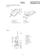
Страница 3: ... SPEAKER 6 Helical antenna 7 FLASH button 8 Dialing keys 9 CHANNEL button º REDIAL PAUSE button PGM Microphone 1 Charging terminals 2 Hang up tab 3 Telescopic antenna 4 POWER CHARGE IN USE lamp BASE UNIT HANDSET This section is extracted from instruction manual 5 PAGE key 6 LINE jack 7 DIAL MODE switch 8 DC IN 9V jack ...

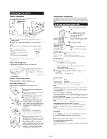
Страница 4: ... 4 ...

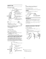
Страница 5: ... 5 ...

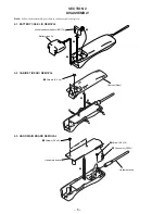
Страница 6: ...ical order given 2 1 BATTERY CASE LID REMOVAL 2 2 CABINET REAR REMOVAL 2 3 HAND MAIN BOARD REMOVAL Battery case lid Nickel cadmium battery BP T16 3 2 1 1 Screws 2 6 x 8 3 3 4 2 2 Cabinet Rear 1 Screws 2 6 x 8 2 Screw 2 6 x 12 4 Connector CN101 3 Hand main board Helical antenna ...

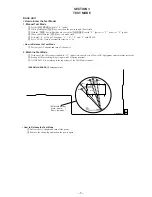
Страница 7: ...How to Release the Test Mode 1 Pull out the AC adapter and turn off the power 2 Machine Test Mode 1 With one of the CH setting terminals in H input state cause Reset of Power ON Equipment enters machine test mode 2 Setting of CH according to logic input with CH setting terminal 3 ON OFF of TX is according to the input logic of the Dial Mode terminal How to Release the Test Mode 1 Pull out the AC a...

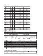
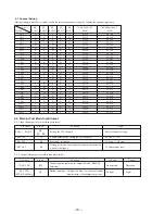
Страница 8: ...760 CH2 L H L L 43 740 48 840 CH3 H H L L 43 820 48 860 CH4 L L H L 43 840 48 920 CH5 43 920 49 020 CH6 43 960 49 080 CH7 44 120 49 100 CH8 44 160 49 160 CH9 44 180 49 200 CH10 44 200 49 240 CH11 44 320 49 280 CH12 44 360 49 360 CH13 44 400 49 400 CH14 H L H L 44 460 49 460 CH15 L H H L 44 480 49 500 CH16 H H H L 46 610 49 670 CH17 L L L H 46 630 49 845 CH18 46 670 49 860 CH19 46 710 49 770 CH20 4...

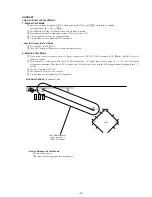
Страница 9: ... When power on reset is applied while a H high is input to the TEST SW TP43 terminal IC501 pin the RING Level H 500msec sounds 2 Following that at a timing in which the TEST SW terminal has H High input there is output of L by the CH Channel setting control terminal Then there is PLL setting to the CH which was read to with the CH setting terminal according to that L output 3 Set the TX setting to...

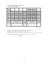
Страница 10: ... H L L 43 920 49 020 CH6 H L H L H 43 960 49 080 CH7 H L H H L 44 120 49 100 CH8 H L H H H 44 160 49 160 CH9 H H L L L 44 180 49 200 CH10 H H L L H 44 200 49 240 CH11 H H L H L 44 320 49 280 CH12 H H L H H 44 360 49 360 CH13 H H H L L 44 400 49 400 CH14 H H H L H 44 460 49 460 CH15 H H H H L 44 480 49 500 CH16 L L H H L 44 610 49 670 CH17 L L H H H 44 630 49 845 CH18 L H L L L 44 670 49 860 CH19 L...

Страница 11: ...tion level and RSSI H sensitivity setting is as follows The following are possible 15 n 44 n 36 36 n 15 n 44 44 n 36 n 15 Upper 4 position 0 1 2 3 7 Lower TX RX RX MIC Lk position RF AF 0 QUIT 10ch 20ch Batt Alarm H A L T G KEY TEST 1 1ch 11ch 21ch CHARG DET G g G G G 2 2ch 12ch 22ch G g g G G 3 3ch 13ch 23ch g g G G G 4 4ch 14ch 24ch RX LOCK g g g G G 5 5ch 15ch 25ch TX LOCK g g g g G 6 6ch 16ch ...

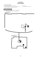
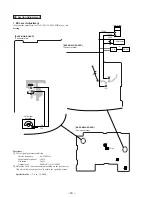
Страница 12: ...10MHz as a rule Set to base unit machine test mode Refer to page 7 TX Section Adjustment Note The electrolytic capacitor 10µF 10V connected TP23 DET OUT to GND Only TX section adjustment Switch position S302 DIAL MODE P pulse JR 7 TP23 10 F FL 101 R212 R206 BASE MAIN BOARD Component side BASE MAIN BOARD Conductor side µ FL101 RV101 ...

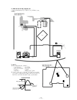
Страница 13: ...justment Procedure 1 The digital voltmeter connected TP5 RX VT to TP19 GND 2 Adjust the L101 for 2 4 0 05V reading on the digital voltmeter CF 101 FL101 CF 101 FL101 IC101 R142 R64 46 TP19 TP19 TP5 TP6 IC101 C135 BASE MAIN BOARD Component side L101 Digital voltmeter TP6 TP19 Digital voltmeter TP5 TP19 BASE MAIN BOARD Conductor side BASE MAIN BOARD Conductor side ...

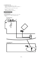
Страница 14: ...SE MAIN BOARD Conductor side TP104 TP105 TP2 TP3 600 Ω or DC 48V F B PBX tester FM rf signal generator level meter Procedure 1 FM rf signal generator condition Carrier frequency 49 910MHz Modulation frequency 1kHz Deviation 3kHz Output level 60dBµV 1mV EMF 2 Adjust the FL101 for the maximum reading on the level meter Also check that the output level is within the specified values Specified value 2...

Страница 15: ...cope to confirm the FM rf signal generator input AF signal waveform and RSSI signal and use the RV101 so that they are synchronized matched duty is synchronized R123 IC101 FL101 TP19 C123 CF101 TP3 C 6 TP2 BASE MAIN BOARD Component side RV101 BASE MAIN BOARD Conductor side TP2 TP3 FM rf signal generator AF oscillator output 20Hz TP9 TP19 oscilloscope DC range TP9 RSSI WAVEFORM RSSI output waveform...

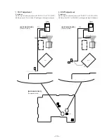
Страница 16: ...o page 9 Setting Set to Handset Test Mode Adjustment Location Hand main board TX Section Adjustment 1 TX VT Adjustment 1 The digital voltmeter connected TP6 TX VT to TP3 GND 2 Adjust the L52 for 1 2V 0 05V reading on the digital voltmeter IC101 47 R64 C66 C65 TP6 TP3 R5 C4 HAND MAIN BOARD Component side L52 Digital voltmeter TP3 TP6 HAND MAIN BOARD Conductor side ...

Страница 17: ...meter connected TP5 RX VT to TP3 GND 2 Adjust the L102 for 0 8V 0 05V reading on the digital voltmeter IC101 46 R130 C142 C141 C61 C136 TP5 TP3 R5 C4 HAND MAIN BOARD Component side L102 Digital voltmeter TP3 TP5 HAND MAIN BOARD Conductor side ...

Страница 18: ...80MHz Modulation 1kHz Deviation 3kHz Output level 60dBµV 1mV EMF 2 Adjust the FL101 for the maximum reading on the level meter Also check that the output level is within the specified values Specified value 16 6 to 8 6dBV TP3 TP2 R5 C4 C11 TP27 TP26 C12 IC101 TP2 TP27 TP26 TP3 FM rf signal generator level meter HAND MAIN BOARD Component side FL101 HAND MAIN BOARD Conductor side ...

Страница 19: ...the oscilloscope to confirm the FM rf signal generator in put AF signal waveform and RSSI signal and use the RV101 so that they are synchronized matched duty is synchronized RSSI WAVEFORM RSSI output waveform RF signal EXT signal 20Hz 0V Adjust so that they synchronize at 0V C113 TP2 TP3 R117 C51 TP9 R506 IC501 HAND MAIN BOARD Component side RV101 HAND MAIN BOARD Conductor side TP2 TP3 FM rf signa...

Страница 20: ...DET I Power failuer DET terminal L Power failure 15 MBR I Make30 40 selection input H 30 L 40 16 PAGE I Page key input H input 17 DIAL MODE I Dial mode selection input terminal 18 CHG DET I Charge DET L Charge 19 RSSI O RSSI sensitivity selection output 20 DP O Dial pulse ON OFF control 21 DTMF O DTMF output terminal 22 TX B CTRL I TX B ON OFF contorl L TX ON 23 M 1 I Channel setting for test mode...

Страница 21: ...T 3 O Intermittent reception activation control L ACT 23 ACT 4 O Intermittent reception activation control L ACT 24 COL 0 I Key scan input terminal 25 COL 1 I Key scan input terminal 26 COL 2 I Key scan input terminal 27 COL 3 I Key scan input terminal 28 MIC O MIC bias output control 29 ROW 1 O Key scan output 30 NC Not used Open 31 ROW 2 O Key scan output terminal 32 ROW 3 O Key scan output term...

Страница 22: ......

Страница 23: ......

Страница 24: ......

Страница 25: ......

Страница 26: ......

Страница 27: ......

Страница 28: ...SHION BUZZER 9 3 935 514 01 CABINET REAR BLACK SPP 800 850 9 3 935 514 11 CABINET REAR CREAM SPP 810 860 10 3 935 515 01 LID BATTERY CASE BLACK SPP 800 850 10 3 935 515 11 LID BATTERY CASE CREAM SPP 810 860 11 3 370 982 01 FOOT H RUBBER 12 3 935 520 01 CUSHION BATTERY 15 3 939 071 01 SPONGE MIC 16 3 939 070 01 TERMINAL ANTENNA ANT1 1 501 839 11 ANTENNA HELICAL HAND BLACK SPP 800 850 ANT1 1 501 839...

Страница 29: ... 163 099 00 CERAMIC CHIP 18PF 5 50V C71 1 163 224 11 CERAMIC CHIP 7PF 0 25PF 50V C101 1 165 319 11 CERAMIC CHIP 0 1uF 50V C102 1 163 239 11 CERAMIC CHIP 33PF 5 50V C103 1 163 106 00 CERAMIC CHIP 36PF 5 50V C105 1 163 243 11 CERAMIC CHIP 47PF 5 50V C106 1 163 137 00 CERAMIC CHIP 680PF 5 50V C107 1 165 319 11 CERAMIC CHIP 0 1uF 50V C108 1 124 907 11 ELECT 10uF 20 50V C109 1 164 232 11 CERAMIC CHIP 0...

Страница 30: ...R 2C 6P LINE PHOTO INTERRUPTER PH201 8 719 156 73 PHOTO COUPLER PS2501 1LA TRANSISTOR Q1 8 729 031 85 TRANSISTOR 2SC4365 34 TB Q51 8 729 031 85 TRANSISTOR 2SC4365 34 TB Q52 8 729 809 77 TRANSISTOR 2SC3142 J4 Q54 8 729 216 22 TRANSISTOR 2SA1162 G Q201 8 729 120 28 TRANSISTOR 2SC1623 L5L6 Q202 8 729 106 68 TRANSISTOR 2SD1615A GP Q301 8 729 106 68 TRANSISTOR 2SD1615A GP Q302 8 729 120 28 TRANSISTOR 2...

Страница 31: ... 10W R506 1 216 049 00 METAL GLAZE 1K 5 1 10W R507 1 216 049 00 METAL GLAZE 1K 5 1 10W R508 1 216 097 00 METAL GLAZE 100K 5 1 10W R509 1 216 121 00 METAL GLAZE 1M 5 1 10W R510 1 216 246 00 METAL GLAZE 100K 5 1 8W R513 1 216 075 00 METAL CHIP 12K 5 1 10W R514 1 216 073 00 METAL CHIP 10K 5 1 10W R515 1 216 057 00 METAL CHIP 2 2K 5 1 10W R522 1 216 097 00 METAL GLAZE 100K 5 1 10W R523 1 216 097 00 ME...

Страница 32: ...RAMIC CHIP 0 1uF 50V C134 1 124 442 00 ELECT 330uF 20 6 3V C136 1 163 237 11 CERAMIC CHIP 27PF 5 50V C137 1 163 009 11 CERAMIC CHIP 0 001uF 10 50V C138 1 163 009 11 CERAMIC CHIP 0 001uF 10 50V C140 1 104 396 11 ELECT 10uF 20 16V C141 1 164 232 11 CERAMIC CHIP 0 01uF 50V C142 1 163 035 00 CERAMIC CHIP 0 047uF 50V C143 1 162 638 11 CERAMIC CHIP 1uF 16V C148 1 163 009 11 CERAMIC CHIP 0 001uF 10 50V C...

Страница 33: ...5 1 10W R69 1 216 057 00 METAL CHIP 2 2K 5 1 10W R101 1 216 093 00 METAL CHIP 68K 5 1 10W R102 1 216 105 00 METAL GLAZE 220K 5 1 10W R103 1 216 105 00 METAL GLAZE 220K 5 1 10W R104 1 216 101 00 METAL GLAZE 150K 5 1 10W R105 1 216 109 00 METAL GLAZE 330K 5 1 10W R106 1 216 049 00 METAL GLAZE 1K 5 1 10W R107 1 216 077 00 METAL CHIP 15K 5 1 10W R108 1 216 097 00 METAL GLAZE 100K 5 1 10W R109 1 216 09...

Страница 34: ...RYSTAL 4 048MHz MISCELLANEOUS 5 1 762 664 11 SWITCH RUBBER KEY BLACK SPP 800 5 1 762 664 21 SWITCH RUBBER KEY CREAM SPP 810 5 1 762 664 31 SWITCH RUBBER KEY BLACK SPP 850 5 1 762 664 41 SWITCH RUBBER KEY CREAM SPP 860 ANT1 1 501 511 11 ANTENNA TELESCOPIC BASE ANT1 1 501 839 11 ANTENNA HELICAL HAND BLACK SPP 800 850 ANT1 1 501 839 21 ANTENNA HELICAL HAND CREAM SPP 810 860 MIC1 1 542 118 11 MICROPHO...

Отзывы: