background image

3

D-FS18

The laser diode in the optical pick-up block may suffer electrostatic
breakdown because of the potential difference generated by the charged
electrostatic load, etc. on clothing and the human body. During repair, pay
attention to electrostatic breakdown and also use the procedure in the printed
matter which is included in the repair parts.
The flexible board is easily damaged and should be handled with care.

NOTES ON LASER DIODE EMISSION CHECK

The laser beam on this model is concentrated so as to be focused on the disc
reflective surface by the objective lens in the optical pick-up block. Therefore,
when checking the laser diode emission, observe from more than 30cm away
from the objective lens.

Before Replacing the Optical pick-up Block

Please be sure to check thoroughly the parameters as per the “Optical pick-
up Block Checking Procedure” (Part No. : 9-960-027-11) issued separately
before replacing the optical Pick-up block.
Note and specifications required to check are given below.

•  FOK output : IC601 

eg

 pin

When checking FOK, remove the lead wire to disc motor.

•  RF signal P-to-P value : 0.4 to 0.5Vp-p

SECTION 1

SERVICING NOTES

NOTES ON HANDLING THE OPTICAL PICK-UP BLOCK OR
BASE UNIT

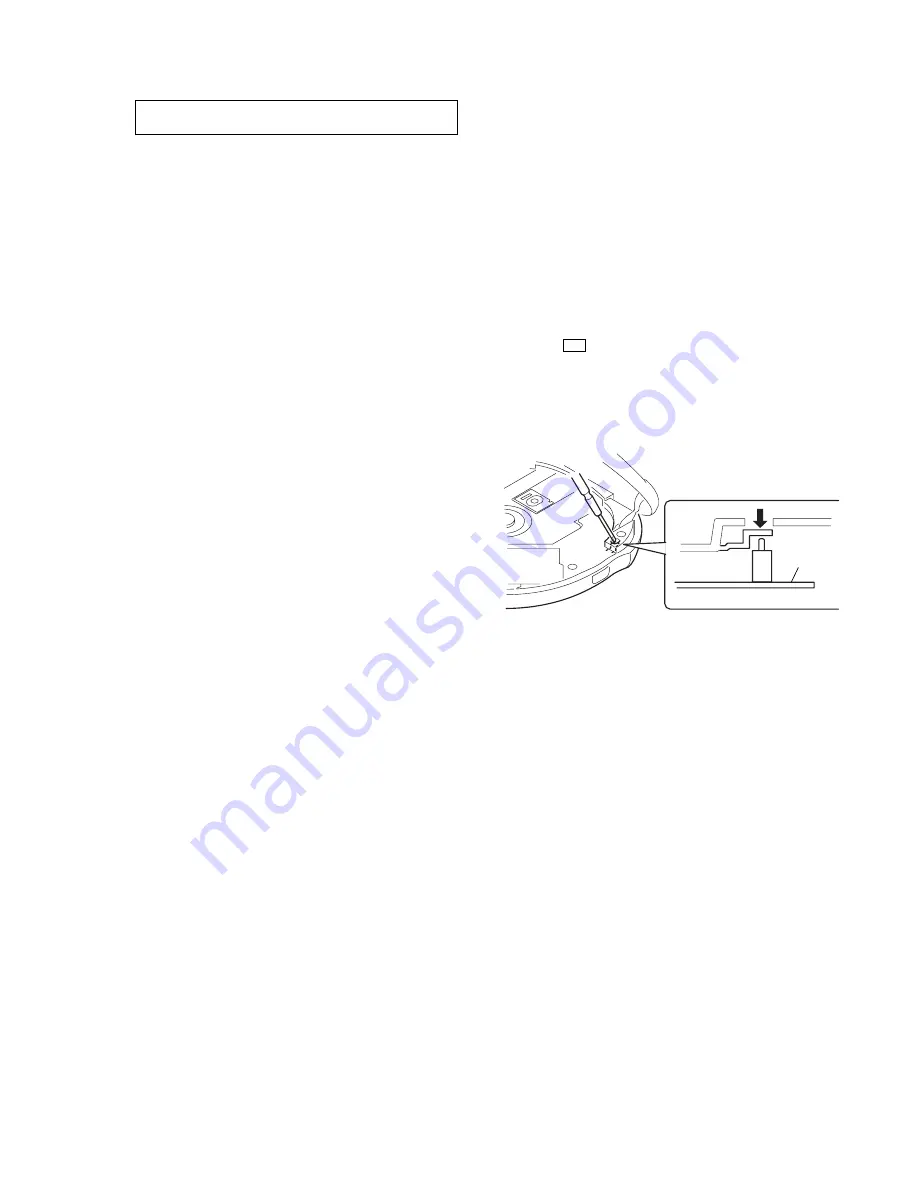
Fig.1 Method to push S801

MAIN board

S801

Precautions for Checking Emission of Laser Diode

Laser light of the equipment is focused by the object lens in the optical
pick-up so that the light focuses on the reflection surface of the disc.
Therefore, be sure to keep your eyes more then 30 cm apart from the object
lens when you check the emission of laser diode.

Laser Diode Checking Methods

During normal operation of the equipment, emission of the laser diode is
prohibited unless the upper lid is closed while turning ON the S801. (push
switch type)
The following two checking methods for the laser diode are oper-able.

• Method:

Emission of the laser diode is visually checked.

1. Open the upper lid.
2. With a disc not set, turn on the S801 with a screwdriver having a thin tip

as shown in Fig.1.

Note:

Do not push the detection lever strongly, or it may be bent or dam-
aged.

3. Press the 

 u

  button.

4. Observing the objective lens, check that the laser diode emits light.

When the laser diode does not emit light, automatic power control circuit
or optical pickup is faulty.
In this operation, the objective lens will move up and down 5 times along
with inward motion for the focus search.

Содержание Sports D-FS18

Страница 1: ... AM Built in ferrite bar antenna General Power requirements For the area code of the model you purchased check the upper left side of the bar code on the package Sony NH WM2AA rechargeable batteries 2 4 V DC Two LR6 size AA batteries 3 V DC AC power adaptor DC IN 4 5 V jack U2 U CA2 E92 MX2 TW2 BR3 model 120 V 60 Hz CED CET CEW CEX CE7 EE EE1 E13 G5 G6 G7 G8 BR1 model 220 230 V 50 60 Hz CEK 3CE7 m...

Страница 2: ...ring Keep the temperature of the soldering iron around 270 C during repairing Do not touch the soldering iron on the same conductor of the circuit board within 3 times Be careful not to apply force on the conductor when soldering or unsoldering Notes on chip component replacement Never reuse a disconnected chip component Notice that the minus side of a tantalum capacitor may be dam aged by heat TA...

Страница 3: ... P to P value 0 4 to 0 5Vp p SECTION 1 SERVICING NOTES NOTES ON HANDLING THE OPTICAL PICK UP BLOCK OR BASE UNIT Fig 1 Method to push S801 MAIN board S801 Precautions for Checking Emission of Laser Diode Laser light of the equipment is focused by the object lens in the optical pick up so that the light focuses on the reflection surface of the disc Therefore be sure to keep your eyes more then 30 cm...

Страница 4: ...phones jack qf Display 5 VOL volume control qs HOLD switch 2 PLAY MODE TUNING button 1 SOUND button 3 REPEAT ENTER TUNING button qd DC IN 4 5 V external power input jack 9 u play pause button 7 Buckle 4 RADIO ON BAND button 8 1 5 buttons q x stop CHG charge RADIO OFF button qa AMS search PRESET buttons ...

Страница 5: ...5 Five screws B2 Cabinet Inner sub assy MAIN board 2Screw tapping 3Screw B2 4Switching arm assy MD ASSY Main board 3 Optical pick up flexible board CN502 Green 2 CN503 White 1 4 3 1 CABINET LOWER SUB ASSY CABINET INNER SUB ASSY MAIN BOARD 3 2 MD ASSY Lid Upper Switch unit Cabinet lower sub ASSY Cabinet inner sub ASSY Main board MD ASSY Motor ASSY Turn table Spindle M902 Optical pick up DAX 23E Mot...

Страница 6: ...ws B1 7x5 Chassis 2 3 5 6 2 1 Screw B 1 7x5 4 Screw P 1 4x3 5 Chassis Optical pick up DAX 23E Bracket Shaft Gear B Cover Gear Motor ASSY Sled M901 Screw feed assy 3 3 MOTOR ASSY TURN TABLE SPINDLE M902 3 4 OPTICAL PICK UP DAX 23E MOTOR ASSY SLED M901 ...

Страница 7: ...7 D FS18 1 4 5 3 2 Lid Upper Switch unit Five screws B 1 7 3 5 Cover Lid 3 5 LID UPPER SWITCH UNIT ...

Страница 8: ...cope to the test points TJ629 RF and TJ635 GND on the MAIN board 2 Set a disc YEDS 18 3 Press the u button 4 Check the oscilloscope waveform is as shown below A good eye pattern means that the diamond shape in the center of the waveform can be clearly distinguished RF Signal reference Waveform Eye Pattern To watch the eye pattern set the oscilloscope to AC range and increase the vertical sensitivi...

Страница 9: ... which enables seeing Note on Schematic Diagrams All capacitors are in µF unless otherwise noted pF µµF 50 WV or less are not indicated except for electrolytics and tantalums All resistors are in Ω and 1 4 W or less unless otherwise specified internal component 2 nonflammable resistor C panel designation H adjustment for repair A B Line Voltages and waveforms are dc with respect to ground under no...

Страница 10: ... XCAS 113 XRAS A0 A10 2 3 24 25 XWE 4 XOE 22 XCAS 23 D0 D3 7 5 3 1 106 109 115 118 111 9 12 15 19 21 8 97 L OUT 104 R OUT 13 A MUTING FM ANT TU R TUMUTE TU L 11 10 9 2 4 14 12 6 13 5 8 1 3 IC302 Q306 Q601 Q305 TUVCC VCC D603 D601 VOLUME RV301 TU BASS1 BEEP O HP Q304 L IN 14 R IN 15 MUTE 19 PWR SW 20 BEEP 17 BB SW 23 BST NF 1 HP AMP IC301 8 L OUT 6 R OUT 24 BST OUT 21 BIAS 2 AD DOUT 10 MIX OUT 11 A...

Страница 11: ...M IN 70 AD DC REF 45 DX O CTR 55 EQ 65 XOUT 74 XIN 75 EEP DO DI 30 EEP SK 31 EEP CS 32 3 DI 4 DO 2 SK 1 CS EEPROM IC62 47 SDO O CDU CD SDI 31 IC801 1 2 SYSTEM CONTROL 46 SDI I CDU CD SDO 32 48 SCK I CDU TUSCK 30 38 TUON TUON 34 28 LCD REQ LCD REQ 33 39 CDON IWP CDU CDON 5 73 RESET XCD RESET TU 29 29 LID OPEN WP OPEN 21 52 XAVLS I SW 51 XHOLD I SW 54 ACK CD ACK CD 19 42 AD1 KEY AD CD KEY 18 HOLD 39...

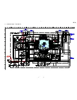
Страница 12: ...IC405 1 2 A B C D E F G H I J 3 4 5 6 7 8 9 10 11 OPTICAL PICK UP BLOCK DAX 23E Ref No Location D403 I 5 D408 I 5 D461 E 6 D601 E 7 IC304 F 3 IC402 E 4 IC404 E 5 IC405 E 10 Q301 G 3 Q403 D 10 Q405 F 4 Q406 H 5 Q407 I 5 Q409 I 5 Q412 E 10 Q413 G 4 Q501 D 3 Semiconductor Location ...

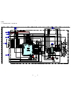
Страница 13: ... 5 D82 E 5 D301 E 9 D302 E 9 D401 D 2 D404 E 3 D405 I 8 D602 F 7 D603 F 7 D804 E 5 IC1 B 6 IC61 C 4 IC62 B 3 IC81 B 3 IC301 F 9 IC302 E 9 IC401 H 8 IC501 D 10 IC601 E 7 IC602 G 6 IC604 D 9 IC801 E 4 Q2 C 6 Q3 B 7 Q4 D 5 Q5 D 5 Q6 B 6 Q8 C 5 Q9 C 5 Q60 C 5 Q84 C 5 Q85 C 4 Q86 F 6 Q302 I 8 Q304 E 10 Q305 E 10 Q306 E 9 Q402 D 2 Q404 F 4 Q408 I 7 Q410 I 8 Q411 G 7 Q414 F 9 Q416 I 9 Q601 D 6 Semiconduc...

Страница 14: ...14 14 D FS18 5 4 SCHEMATIC DIAGRAM TUNER SECTION IC B D ...

Страница 15: ...15 15 D FS18 5 5 SCHEMATIC DIAGRAM CD SECTION 1 4 ...

Страница 16: ...16 16 D FS18 5 6 SCHEMATIC DIAGRAM CD SECTION 2 4 IC B D ...

Страница 17: ...17 17 D FS18 5 7 SCHEMATIC DIAGRAM CD SECTION 3 4 IC B D ...

Страница 18: ...18 18 D FS18 5 8 SCHEMATIC DIAGRAM CD SECTION 4 4 IC B D ...

Страница 19: ...input Analog VDD for A D signal input Power supply terminal 2V Sub code sync S0 S1 detection signal input from the IC601 GRSCOR signal input from the IC601 H MIRX series L MISX Beep sound output to the headphone amplifier IC302 DTS pull up 200K Communication clock output to the communication format converter IC802 Serial data out to DTS Serial data in to DTS LCD buty data send request signal outpu...

Страница 20: ... O O I O O I I Description Not usde Not usde Auto Test terminal for IC Fixed at L Not usde Not usde System reset signal input from the power control IC401 L reset System clock input terminal Not usde Pin Name V3 V1 C1 C0 STOP ICTEST NC NC RESET I XIN I XOUT ...

Страница 21: ...use Vdd as ref 5 keys Not used TU On request CD ON request Weakup TU in sleep mode Reserved Not used Set Keys Remote Key Battery HiDC Level detect use VEE1 55 or 3 3V external Ref DC of A D use for HiDC and batt detects keys vol and RMkeys use VDD as ref Serial input from CD micon Serial output to CD micon reserved line Not use Serial clock to CD micon Beep sound control Not used HOLD detect AVLS ...

Страница 22: ...M IF input PLL error output Not used Not used Not used IC System GND FM OSC in AM OSC in VDD power supply 3 0V Power reset Resset by CD Micon Crystal Osc pin Crystal Osc pin Crystal Osc pin LCD voltage doubler LCD voltage doubler LCD voltage doubler Constant voltage for LCD 1 55V Pin Name B ON OFF IFREQ O TUMUTE O TEST IFIN EO NC HOLD NC GND FMIN AMIN VDD RESET XOUT XIN VXT VLCD C1 C2 VEE ...

Страница 23: ... LED IF REQ DET OUT LPF1 LPF2 FM OSC AM OSC AM MIX FM MIX BUFF BUFF FM RF AMIF FMIF AGC MUTE ST MO FM AM FM DET AM DET 1 8 LEVEL DET IF BUFF AF BUFF AF IF REQ SW ST 23 20 19 18 17 16 15 14 13 2 3 4 5 6 7 8 9 10 11 12 1 24 BIAS BEEP PW SW MT SW ALC DET ATT SW PWC SW OUT B OUT A BEEP IN BST PW B PW C BST NF ADD OUT RF IN PWC SW OUT B OUT C OUT A PWR GND MIX OUT ALC IN ALC DET ATT SW IN A IN B GND MT...

Страница 24: ...2 RI2 RS RF4 DCIN VCPU VCC1 RSTB DTC2D DTC1D INM1 RF1 BATM2 BATM1 INP1 INM4 CHGSW CHGMNT MGND4 MGND3 MGND2 MGND1 VD34 VD23 VD12 VLGO1 VLGO2 VLG3 L1L L1H L2H L2L L3 PGND1 PGND2 PGND3 VIN INP3 INM3 RF3 RF21 DTC3 PAPC VINDET VREF L4 VG GND SYNC CLOCK DATA LATCH HIPC HPI2 HPI1 FR4 RI3 FI3 PWM4 STNG N C WAKE UP RF2 INM2 PWM H P DRIVER H BRIDGE DRIVER4 H BRIDGE DRIVER3 H BRIDGE DRIVER2 H BRIDGE DRIVER1 ...

Страница 25: ...C176 MDP MDS SSTP SFDR SRDR TFDR TRDR FFDR FRDR FRDR FFDR TRDR TFDR SRDR SFDR SCLK ATSK SSTP COUT FOK DFCT MIRR VSS1 TEST TES1 AVDD0 IGEN AVSS0 RFDC E F 120 119 118 117 116 115 114 113 112 111 110 109 108 107 106 105 104 103 102 101 100 99 98 97 96 95 94 93 92 91 XOE XCAS D2 D3 D0 D1 XWE XRAS A11 A10 DVDD A0 A1 A2 A3 AVDD2 LOUT2 AIN2 AOUT2 AVSS2 AVSS1 AOUT1 AIN1 LOUT1 AVDD1 XVSS XTAO XTAI XVDD BCK...

Страница 26: ...EW B2 2 X 3380 333 1 BUCKLE SUB ASSY 3 X 3380 572 1 BRACKET ROLLER ASSY 4 3 338 687 21 SCREW M1 4X2 TAPPING 5 3 343 254 41 SCREW B1 7X3 5 TAPPING 6 3 225 157 01 COVER LID 7 1 476 429 11 SWITCH UNIT 8 3 221 301 01 PACKING UPPER LID 9 3 224 858 01 SPACER 10 3 224 719 01 SPACER C 11 3 225 462 01 SPACER D 12 X 3379 446 1 CABINET INNER ASSY 13 4 908 792 71 SCREW B2 14 4 222 765 01 INSULATOR 15 3 047 19...

Страница 27: ... 61 4 218 827 01 BRACKET SHAFT 62 3 686 458 03 SCREW P1 4X3 5 TAPPING 063 X 4952 506 1 OPTICAL PICK UP DAX 23E M901 A 3328 627 A MOTOR ASSY SLED WITH GEAR M902 A 3328 759 A MOTOR ASSY TURN TABLE SPINDLE The components identified by mark 0 or dotted line with mark 0 are critical for safety Replace only with part number specified Les composants identifiés par une marque 0 sont critiques pour la sécu...

Страница 28: ...3V C32 1 164 362 11 CERAMIC CHIP 470PF 5 00 50V C33 1 162 970 11 CERAMIC CHIP 0 01uF 10 25V C34 1 162 953 11 CERAMIC CHIP 100PF 5 50V C35 1 104 852 11 TANTAL CHIP 22uF 20 00 6 3V C36 1 162 970 11 CERAMIC CHIP 0 01uF 10 25V C39 1 162 970 11 CERAMIC CHIP 0 01uF 10 25V C40 1 162 970 11 CERAMIC CHIP 0 01uF 10 25V C41 1 162 927 11 CERAMIC CHIP 100PF 5 50V C45 1 162 970 11 CERAMIC CHIP 0 01uF 10 25V C46...

Страница 29: ...CHIP 68PF 5 00 50V C501 1 164 156 11 CERAMIC CHIP 0 1uF 25V C502 1 117 720 11 CERAMIC CHIP 4 7uF 10V C504 1 125 838 11 CERAMIC CHIP 2 2uF 10 6 3V C505 1 115 156 11 CERAMIC CHIP 1uF 10V C506 1 162 927 11 CERAMIC CHIP 100PF 5 50V C507 1 162 925 11 CERAMIC CHIP 68PF 5 00 50V C508 1 125 838 11 CERAMIC CHIP 2 2uF 10 6 3V C602 1 115 467 11 CERAMIC CHIP 0 22uF 10 00 10V C603 1 107 826 11 CERAMIC CHIP 0 1...

Страница 30: ... 1 754 168 11 ANTENNA FERRITE ROD MW L4 1 406 404 11 COIL MW OSCILATION L5 1 414 410 21 INDUCTOR 10uH L62 1 412 006 31 INDUCTOR 10uH L80 1 412 006 31 INDUCTOR 10uH L321 1 414 756 11 INDUCTOR 47uH L401 1 419 188 11 INDUCTOR 100uH L402 1 414 754 11 INDUCTOR 10uH L403 1 414 434 11 INDUCTOR 100uH L404 1 414 757 11 INDUCTOR 100uH L405 1 414 757 11 INDUCTOR 100uH L406 1 414 404 11 INDUCTOR 100uH L407 1 ...

Страница 31: ...0K 5 1 16W R106 1 216 841 11 METAL CHIP 47K 5 1 16W R107 1 218 975 11 RES CHIP 68K 5 1 16W R108 1 216 809 11 METAL CHIP 100 5 1 16W R121 1 216 864 11 METAL CHIP 0 5 1 16W R124 1 216 793 11 RES CHIP 4 7 5 1 16W R202 1 216 839 11 METAL CHIP 33K 5 1 16W R203 1 218 871 11 METAL CHIP 10K 0 5 1 16W R204 1 216 833 11 METAL CHIP 10K 5 1 16W R206 1 216 841 11 METAL CHIP 47K 5 1 16W R207 1 218 975 11 RES CH...

Страница 32: ...TAL CHIP 680 5 1 16W R632 1 218 971 11 RES CHIP 33K 5 1 16W R634 1 216 809 11 METAL CHIP 100 5 1 16W R635 1 216 864 11 METAL CHIP 0 5 1 16W R644 1 218 977 11 RES CHIP 100K 5 1 16W R647 1 218 951 11 RES CHIP 680 5 1 16W R648 1 216 819 11 METAL CHIP 680 5 1 16W R649 1 218 951 11 RES CHIP 680 5 1 16W R652 1 216 831 11 METAL CHIP 6 8K 5 1 16W R653 1 216 841 11 METAL CHIP 47K 5 1 16W R654 1 216 847 11 ...

Страница 33: ...CESSORIES PACKING MATERIALS 0 1 467 009 21 ADAPTOR AC AC E455D 3 221 356 01 STRAP HAND 3 226 007 11 MANUAL INSTRUCTION ENGLISH US 3 226 008 11 MANUAL INSTRUCTION FRENCH CND 3 226 008 21 MANUAL INSTRUCTION ENGLISH CND 8 953 284 93 HEADPHONE MDR W014LPY1K SET The components identified by mark 0 or dotted line with mark 0 are critical for safety Replace only with part number specified Les composants ...

Страница 34: ...ORY Clicking the version allows you to jump to the revised page Also clicking the version at the upper right on the revised page allows you to jump to the next revised page Ver Date Description of Revision 1 0 2001 04 New ...

Отзывы: