background image

– 35 –

(1)

MAIN  SECTION

SECTION  7

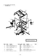
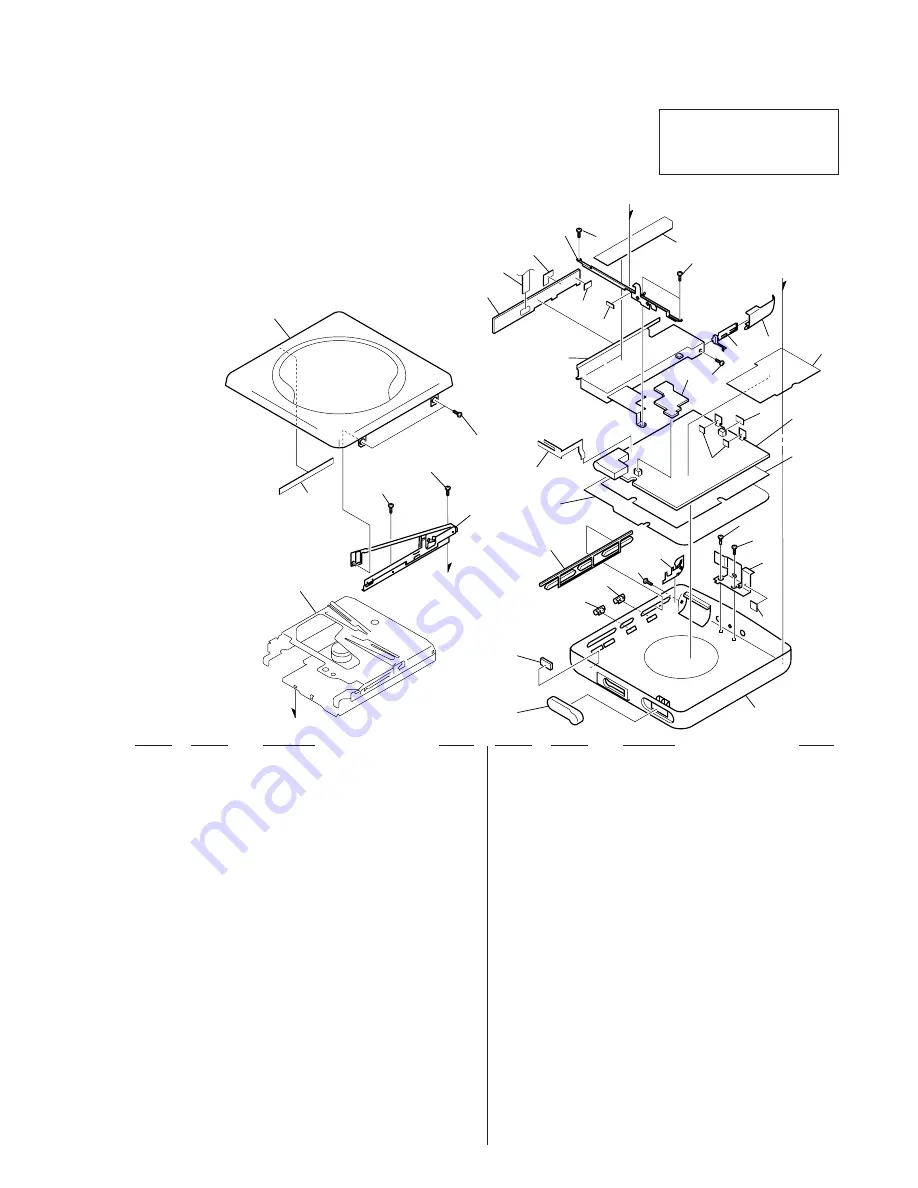
EXPLODED  VIEWS

The components identified by
mark 

!

 or dotted line with mark

!

 are critical for safety.

Replace only with part number
specified.

• Items marked “*” are not stocked since they

are seldom required for routine service. Some
delay should be anticipated when ordering
these items.

• The mechanical parts with no reference num-

ber in the exploded views are not supplied.

• Accessories and packing materials are given

in the last of the electrical parts list.

NOTE:

• -XX and -X mean standardized parts, so they

may have some difference from the original
one.

• Color Indication of Appearance Parts

Example:
KNOB, BALANCE (WHITE) . . . (RED)

Parts Color Cabinet's Color

Ref. No.

Part No.

Description

Remark

Ref. No.

Part No.

Description

Remark

12

1

7

24

15

23

34

22

10

13

17

A

A

B

2

21

9

6

36

4

8

29

5

33

31

30

11

2

3

MT-MZE55-150

35

14

18

14

16

12

19

32

20

B

26

27

28

25

1

4-219-842-01 KNOB, OPEN

2

4-963-883-21 SCREW (M1.4), PRECISION PAN

3

X-4951-977-1 LID ASSY (S), UPPER (SILVER)

3

X-4951-978-1 LID ASSY (S), UPPER (BLUE)

3

X-4951-979-1 LID ASSY (S), UPPER (BLACK)

4

X-4951-974-1 PANEL ASSY (S), BOTTOM (SILVER)

4

X-4951-975-1 PANEL ASSY (S), BOTTOM (BLUE)

4

X-4951-976-1 PANEL ASSY (S), BOTTOM (BLACK)

5

3-349-825-21 SCREW

6

4-223-224-01 SHEET (PANEL) (BLUE)

6

4-223-224-11 SHEET (PANEL) (SILVER)

6

4-223-224-21 SHEET (PANEL) (BLACK)

7

4-212-895-01 TERMINAL BOARD (MINUS)

8

4-214-158-01 DAMPER (-)

9

A-3322-066-A SW BOARD, COMPLETE

10

1-674-262-11 SWITCH FLEXIBLE BOARD

11

X-4951-549-1 SLIDER ASSY, OPEN

12

3-015-033-01 SCREW (B1.4X3), TAPPING

13

4-213-092-01 LABEL, CAUTION

14

3-895-823-01 SCREW (B1.4X2.3), TAPPING

15

4-219-834-01 CASE, BATTERY

16

4-223-757-01 SHEET (SLIDER)

17

A-3322-068-A AUDIO BOARD, COMPLETE

18

X-4950-411-1 TERMINAL (PLUS) ASSY, BATTERY

19

4-222-800-01 SCREW (1.4X2)

20

X-4951-548-1 PLATE (R) ASSY, FULCRUM

21

4-219-833-01 LID, BATTERY CASE (BLUE)

21

4-219-833-11 LID, BATTERY CASE (SILVER)

21

4-219-833-21 LID, BATTERY CASE (BLACK)

22

4-212-871-01 SHEET, BLIND

23

A-3323-244-A MAIN BOARD, COMPLETE

24

4-219-843-01 BRACKET (CASE)

25

4-219-840-01 KNOB (MB) (BLUE)

25

4-219-840-11 KNOB (MB) (SILVER)

25

4-219-840-21 KNOB (MB) (BLACK)

26

4-219-836-01 KNOB (AVLS) (BLUE)

26

4-219-836-11 KNOB (AVLS) (SILVER)

26

4-219-836-21 KNOB (AVLS) (BLACK)

27

4-219-835-01 BUTTON, CONTROL

28

X-4951-964-1 PLATE (L) ASSY, FULCRUM

29

4-223-563-01 SHEET (CHASSIS)

30

4-223-564-01 SHEET (CONTROL), CONDUCTIVE

31

4-223-223-01 SHEET (TERMINAL)

32

4-223-221-01 SHEET (BRACKET)

33

4-223-756-01 SHEET (OPEN)

34

4-223-222-01 SHEET, CONDUCTIVE

35

3-890-155-01 PAN (DIA. 1.4)

36

4-224-063-01 SHEET

Содержание MZ-E80

Страница 1: ...t Model Model Name Using Similar Mechanism MZ E55 Mechanism Type MT MZE55 150 Optical Pick Up Name ODX 1B SPECIFICATIONS MZ E80 US and foreign patents licensed from Dolby Laboratories Licensing Corporation Photo Silver Ver 1 1 2000 05 With SUPPLEMENT 1 9 927 132 82 ...

Страница 2: ...OMPONENT WARNING COMPONENTS IDENTIFIED BY MARK OR DOTTED LINE WITH MARK ON THE SCHEMATIC DIAGRAMS AND IN THE PARTS LIST ARE CRITICAL TO SAFE OPERATION REPLACE THESE COMPONENTS WITH SONY PARTS WHOSE PART NUMBERS APPEAR AS SHOWN IN THIS MANUAL OR IN SUPPLEMENTS PUB LISHED BY SONY CAUTION Use of controls or adjustments or performance of procedures other than those specified herein may result in hazar...

Страница 3: ...uttons FF PLAY REW p STOP 8 External battery terminal 9 OPEN switch º 2 REMOTE jack 1 Headphone 2 MD operate switch PLAY FF REW 3 VOL buttons 4 Display window 5 DISPLAY button 6 PLAYMODE button 7 P PAUSE button 8 HOLD c switch 9 p STOP button 8 7 6 5 4 3 2 1 0 9 8 7 6 5 4 3 2 1 9 LOCATION OF CONTROLS Main Unit Remote commander with headphone ...

Страница 4: ...55 150 SW board Main Board Audio board Optical pick up section This set can be disassembled in the order shown below 5 two screws M1 4 1 6 6 fulcrum plate L assy main section 7 upper lid assy 1 knob open 2 4 screw M1 4 1 3 3 lid battery case 1 screw B1 4 3 1 two screws B1 4 2 3 2 Open slider assy main board main section 5 mechanism deck section 4 flexible board CN501 3 flexible board CN551 ...

Страница 5: ...1 4 2 3 SW board 2 flexible board 1 caution label 2 battery case main board 1 Note In removing the Audio board raise the connector section uprightly 2 Note If the SW board or flexible board is removed the caution label 4 213 092 01 on the flex ible board will be defaced or deformed and replace it with a new label 2 flexible board 4 optical pick up section 3 screw M1 4 2 5 chassis assy 1 flexible b...

Страница 6: ...ode was entered by shorting the test point turn off the power and open the solder bridge of TAP805 TEST MODE on the MAIN board Operation of Setting on Test Mode When the test mode is set the LCD displays the following The cycle the above ROM version display n All lit n All off is repeated When the PLAYMODE key is pressed and hold down the dis play at that time is held so that display can be checke...

Страница 7: ... mode 2 Description of Each Mode 010 Offset adjustment Mode Description 011 VC offset FE offset ABCD offset 012 Not used 013 Not used 014 Not used 020 Laser power adjustment Mode Description 021 MO power GRV 022 MO power LPIT 023 CD power HPIT 024 Not used 030 MO adjustment Mode Description 031 MO EF balance 032 MO tracking offset 033 MO ABCD gain 034 MO focus gain 035 MO tracking gain 036 MO focu...

Страница 8: ...search 072 Access 32 073 Not used 074 Not used 090 NV relation Mode Description 091 NV clear 092 Power OFF 093 Function code change Note The parenthesizal mode numbers in table are not displayed on the LCD of remote commander Audio Mode Enter the test mode and press the VOL key Then press the key and the VOL key in this turn to enter audio mode When entering another mode refer to the configuration...

Страница 9: ...st mode and press the VOL key Then press the key and the VOL key in this turn to enter power mode When entering another mode refer to the configuration of test mode 1 Structure of Power Mode Overall Adjustment Mode Enter the test mode and press the VOL key to enter overall adjustment mode When entering another mode refer to the configuration of test mode When the overall adjustment mode is entered...

Страница 10: ...led out 3 071 Focus search 4 031 MO EF balance 5 033 MO ABCD gain 6 031 MO EF balance 7 032 MO tracking offset 8 034 MO focus gain 9 035 MO tracking gain 10 036 MO focus bias Remote commander display during automatic adjustment 4 If result of automatic adjustment is OK the following display appears 5 If result of automatic adjustment is NG the following display appears If NG enter servo mode to pe...

Страница 11: ...QUENCOR SPINDLE SERVO PWM GENERATOR 127 128 129 130 131 132 138 139 DIGITAL SERVO SIGNAL PROCESS 113 45 46 47 38 39 42 24 37 1 BGR 19 TRACKING VOLTAGE MONITOR IC502 27 28 52 65 66 64 67 56 57 58 69 EEPROM IC802 9 76 75 74 73 7 1 2 3 4 PE CS BK DI DO 20 19 OSCILLATOR CELL 27 24 34 38 45 43 46 42 33 31 23 51 29 30 17 16 8 S804 808 44 69 6 68 34 63 7 71 70 60 21 22 15 BEEP 24 23 2 4 17 18 13 HEADPHON...

Страница 12: ......

Страница 13: ...taken with a oscilloscope Voltage variations may be noted due to normal produc tion tolerances Circled numbers refer to waveforms Signal path E PLAYBACK Note The components identified by mark or dotted line with mark are critical for safety Replace only with part number specified IC601 is not replaceable The voltage and waveform of CSP chip size package can not be measured because its lead layout ...

Страница 14: ... DRIVER PRE DRIVER PWM DRIVER VC VC VG VC VC VG VC VC VG VC VC VG VC VC VG VC VC VG VC VC VG VC VG VG VG VG VG VC VC VC VC REN ROE 1ntSTB 1ntSTB 1ntOE DO or DI F12 R12 F11 R11 R13 F13 R14 F14 OE VREG VREG CONT CLPF RGND VC GND VG PWM DI DO VB1 VB1 VB VB VB2 LI LI UO VO WO V0 V0 L2H L2L GND DCC2 GND DCC1 GND DCC1 HIU HIV HIW P11 P12 VPS2 PO2 GND PS PO1 VPS1 GND 3P2 HOW VD2 HOV GND 3PI HOU VD IN GND...

Страница 15: ...C CONVERTER PWM1 MODE SELECT SAW OSC2 XWK1 XWK2 XWK3 XWK4 FFCLR SLEEP VBSEL CLK VB2 VB1 PGND SW PWMI DO DI VCON 1 2 3 CHIP ENABLE VREF 2STEP PFM CONTROL OSC 100 180kHz VLX LIMITER 5 4 VDD CE VOUT NC VSS LX BUFFER AUDIO Board IC301 TA2131FL EL V REF MT SW BST SW BEEP 19 20 21 22 23 24 18 17 16 15 14 13 PW SW 12 11 10 8 7 BST1 9 BST2 6 5 4 3 2 1 BST AGC PW B PW A ADD MT TC VCC1 INB INA BEEP OUTB BEE...

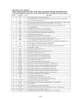
Страница 16: ...ircuit BPF3T 24 VCC Power supply terminal 2 4V 25 WBLADJ I Center frequency setting terminal for the internal circuit BPF22 26 TE O Tracking error signal output to the CXD2663GA IC601 27 CSLED I Connected to the capacitor for low pass filter of the sled error signal 28 SE O Sled error signal output to the CXD2663GA IC601 29 ADFM O FM signal output terminal of the ADIP 30 ADIN I Receives a ADIP FM ...

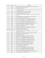
Страница 17: ...17 TST2 I Input terminal for the test fixed at L 18 VDIOSC Power supply terminal 2 4V for oscillator cell 19 OSCI I System clock 512Fs 22 5792 MHz input terminal 20 OSCO O System clock 512Fs 22 5792 MHz output terminal 21 VSIOSC Ground terminal for oscillator cell 22 DAVSSL Ground terminal for internal D A converter L ch 23 VREFL O Reference voltage output terminal for internal D A converter L ch ...

Страница 18: ...tput terminal 75 ASYI I Playback EFM asymmetry comparator voltage input terminal 76 AVD1 Power supply terminal 2 4V analog system 77 BIAS I Playback EFM asymmetry circuit constant current input terminal 78 RFI I Playback EFM RF signal input from the CXA2523ATQ IC501 79 AVS1 Ground terminal analog system 80 PCO O Phase comparison output for master clock of the recording playback FEM master PLL 81 F...

Страница 19: ...al output terminal Not used open 119 FGIN I FG signal input terminal for spindle servo 120 to 122 TEST1 to TEST3 I Input terminal for the test normally fixed at L 123 MTFLGR O Muting applied to analog signal input in non signal status causes the signal to be H automatically Not used 124 SPVS O Spindle servo drive voltage control signal output to the MPC17A55VF IC551 125 VDI03 Power supply terminal...

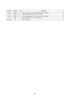
Страница 20: ...ower supply terminal 2 4V for internal 16M bit D RAM 145 DVSS1 Ground terminal for internal 16M bit D RAM 146 DVDD1 Power supply terminal 2 4V for internal 16M bit D RAM 147 TST8 I Input terminal for the test Not used open 148 to168 NC Not used open ...

Страница 21: ...D Power supply terminal 2V digital system 22 VSS Ground terminal digital system 23 HOLD SW I HOLD switch S802 input terminal L hold off H hold on 24 XRFSW O Standby control signal output to the CXA2523ATQ IC501 L standby 25 26 NC Not used open 27 SQSY I Subcode Q sync SCOR input from the CXD2663GA IC601 L is input every 13 3 msec Almost all H is input 28 XINT I Interrupt status input from the CXD2...

Страница 22: ... trigger edge input from the the CXD2663GA IC601 H edge detectable 60 BEEP O Beep sound drive signal output to the headphone amplifier IC301 61 VSS Ground terminal digital system 62 SPCK O Not used open 63 RMC DTCK I O TSB serial communication data input output terminal for remote commander with headphone 64 SCLK O Serial clock signal output to the CXD2663GA IC601 65 SRDT I Reading data input from...

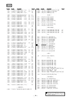
Страница 23: ...51 976 1 PANEL ASSY S BOTTOM BLACK 5 3 349 825 21 SCREW 6 4 223 224 01 SHEET PANEL BLUE 6 4 223 224 11 SHEET PANEL SILVER 6 4 223 224 21 SHEET PANEL BLACK 7 4 212 895 01 TERMINAL BOARD MINUS 8 4 214 158 01 DAMPER 9 A 3322 066 A SW BOARD COMPLETE 10 1 674 262 11 SWITCH FLEXIBLE BOARD 11 X 4951 549 1 SLIDER ASSY OPEN 12 3 015 033 01 SCREW B1 4X3 TAPPING 13 4 213 092 01 LABEL CAUTION 14 3 895 823 01 ...

Страница 24: ...82 555 01 GEAR A 59 4 965 893 01 WASHER GEAR A STOPPER 60 4 986 811 01 SPRING EJECT TENSION 61 X 4948 793 1 LEAD ASSY 62 4 212 899 01 SPRING THRUST 63 X 4949 164 1 OPTICAL PICK UP ASSY ODX 1B 64 4 214 478 01 SHAFT MAIN 65 4 214 207 01 SHEET OP 66 4 222 799 01 SPACER OP FLEXIBLE M501 8 835 594 02 MOTOR DC SSM 01C03A C N SPINDLE M502 1 698 764 21 MOTOR SLED SLED M502 M501 51 52 52 53 54 55 56 57 58 ...

Страница 25: ...510 1 162 965 11 CERAMIC CHIP 0 0015uF 10 50V C511 1 162 967 11 CERAMIC CHIP 0 0033uF 10 50V C512 1 115 467 11 CERAMIC CHIP 0 22uF 10 10V C513 1 107 826 11 CERAMIC CHIP 0 1uF 10 16V C514 1 162 969 11 CERAMIC CHIP 0 0068uF 10 25V C515 1 107 826 11 CERAMIC CHIP 0 1uF 10 16V C516 1 127 569 11 TANTALUM CHIP 100uF 20 4V C518 1 127 569 11 TANTALUM CHIP 100uF 20 4V C519 1 165 176 11 CERAMIC CHIP 0 047uF ...

Страница 26: ...MIC CHIP 0 1uF 10 16V C907 1 107 826 11 CERAMIC CHIP 0 1uF 10 16V C908 1 109 982 11 CERAMIC CHIP 1uF 10 10V C910 1 162 970 11 CERAMIC CHIP 0 01uF 10 25V C911 1 135 259 11 TANTALUM CHIP 10uF 20 6 3V C912 1 135 259 11 TANTALUM CHIP 10uF 20 6 3V C918 1 164 156 11 CERAMIC CHIP 0 1uF 25V C919 1 164 156 11 CERAMIC CHIP 0 1uF 25V C920 1 164 156 11 CERAMIC CHIP 0 1uF 25V CONNECTOR CN301 1 750 316 31 CONNE...

Страница 27: ... 216 845 11 METAL CHIP 100K 5 1 16W R802 1 216 845 11 METAL CHIP 100K 5 1 16W R803 1 216 853 11 METAL CHIP 470K 5 1 16W R804 1 216 833 11 RES CHIP 10K 5 1 16W R805 1 216 853 11 METAL CHIP 470K 5 1 16W R806 1 218 895 11 RES CHIP 100K 0 5 1 16W R807 1 218 895 11 RES CHIP 100K 0 5 1 16W R808 1 216 825 11 METAL CHIP 2 2K 5 1 16W R811 1 216 827 11 METAL CHIP 3 3K 5 1 16W R812 1 216 841 11 METAL CHIP 47...

Страница 28: ...L UNIT RM MZE1 1 528 580 21 BATTERY CHARGER BC 7HT Tourist 1 528 842 11 BATTERY NICKEL HYDROGEN 1 528 866 11 BATTERY CHARGER BC 9HP2 Hong Kong 1 569 007 11 ADAPTOR CONVERSION 2P Tourist 1 759 628 21 CASE BATTERY 3 008 521 21 CASE BATTERY CHARGE 3 867 258 11 MANUAL INSTRUCTION JAPANESE KOREAN Tourist 3 867 258 21 MANUAL INSTRUCTION ENGLISH CHINESE 3 867 258 31 MANUAL INSTRUCTION FRENCH SPANISH Tour...

Страница 29: ...674 352 12 MAIN BOARD Conductor Side AUDIO BOARD Component Side SWITCH BOARD Conductor Side ECN DA800895 DA800972 The MAIN board AUDIO board and SW board have been changed in the middle of production Printed wiring board and schematic diagram of new type and changed parts list are described in this Supplement 1 Refer to original service manual 9 927 132 S previously issued for other information Wh...

Страница 30: ... C920 R912 C832 C831 C308 C619 R540 C525 C524 C809 R819 R613 R607 C611 C610 C609 C527 R606 MAIN BOARD COMPONENT SIDE 1 674 351 12 12 1 674 351 12 12 1 674 263 12 12 1 674 263 12 12 12 12 C911 C564 C565 C912 C558 C553 C554 C556 C555 C908 D901 D903 A K A K C904 C557 C573 C568 C559 C574 C560 C621 C501 C502 C603 C509 C561 C572 C570 C562 C563 C569 B C E Q551 Q552 D902 B C E Q502 B C E Q901 Q903 Q902 G ...

Страница 31: ...th respect to ground under no signal conditions no mark PLAYBACK Voltages are taken with a VOM Input impedance 10 MΩ Voltage variations may be noted due to normal produc tion tolerances Waveforms are taken with a oscilloscope Voltage variations may be noted due to normal produc tion tolerances Circled numbers refer to waveforms Signal path E PLAYBACK Note The components identified by mark 0 or dot...

Страница 32: ... 164 156 11 CERAMIC CHIP 0 1uF 25V CONNECTOR CN301 1 750 316 31 CONNECTOR BOARD TO BOARD 10P CN501 1 778 168 11 CONNECTOR FFC FPC ZIF 20P CN551 1 793 124 21 CONNECTOR FPC ZIP 8P CN801 1 793 327 21 CONNECTOR FPC ZIF 9P DIODE D151 8 719 017 58 DIODE MA8068 D251 8 719 017 58 DIODE MA8068 D351 8 719 017 58 DIODE MA8068 D802 8 719 056 54 DIODE MAZS068008SO D803 8 719 056 54 DIODE MAZS068008SO D804 8 71...

Отзывы: