background image

MICROFILM

SERVICE MANUAL

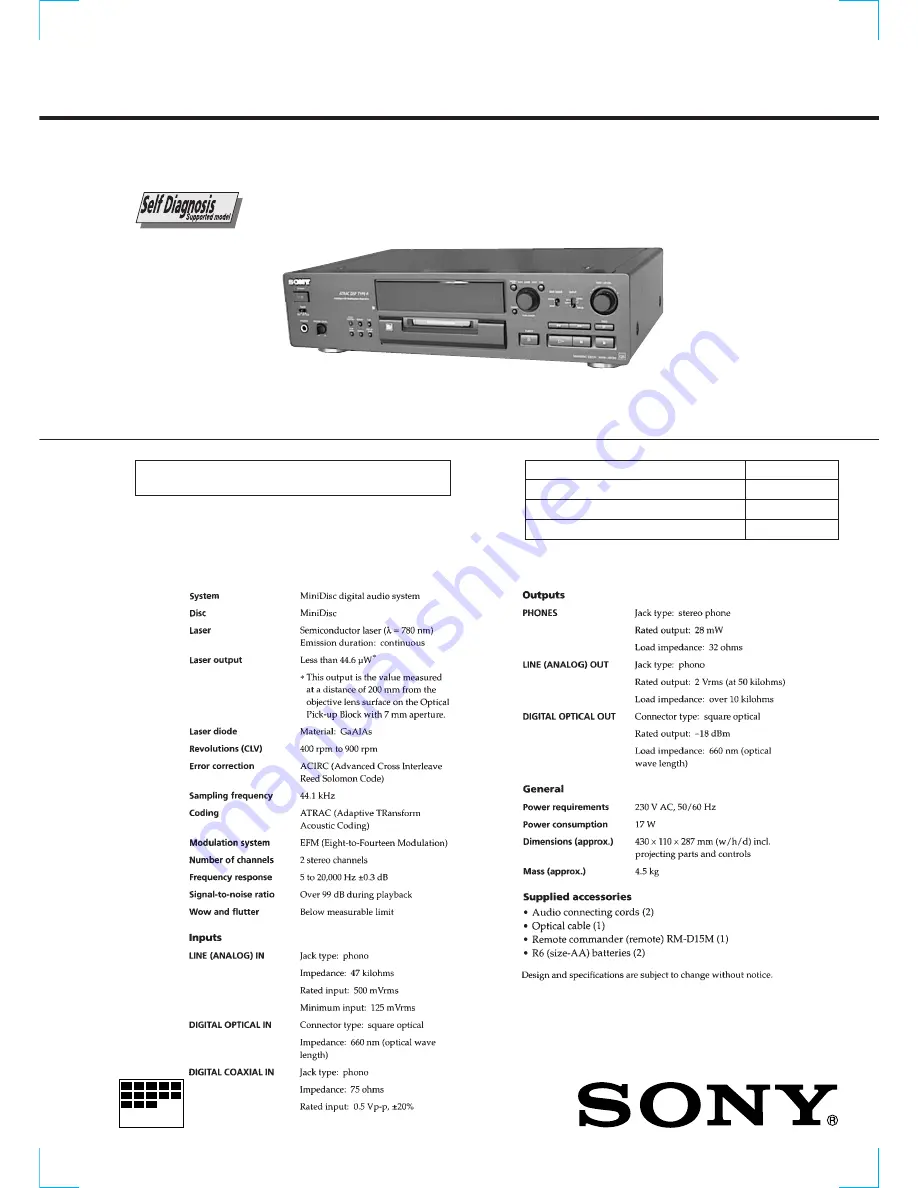
MINIDISC DECK

AEP Model

UK Model

SPECIFICATIONS

MDS-JB730

Model Name Using Similar Mechanism

MDS-JE520

MD Mechanism Type

MDM-5D

Base Unit Type

MBU-5D

Optical Pick-up Type

KMS-260B/J1N

U.S. and foreign patents licensed form Dolby Laboratories
Licensing Corporation.

Содержание MDS-JB730

Страница 1: ...Model UK Model SPECIFICATIONS MDS JB730 Model Name Using Similar Mechanism MDS JE520 MD Mechanism Type MDM 5D Base Unit Type MBU 5D Optical Pick up Type KMS 260B J1N U S and foreign patents licensed form Dolby Laboratories Licensing Corporation ...

Страница 2: ...cribes the least required procedure Be careful not to enter other modes by mistake If you set other modes accidentally press the MENU NO button to exit the mode 1 While pressing the AMS knob and p button connect the power plug to the outlet and release the AMS knob and p button 2 Turn the AMS knob and when Service is displayed press the YES button 3 Turn the AMS knob to display ERR DP MODE 4 Press...

Страница 3: ...s 0π E π indicates the history number The smaller the number the more recent is the error 00 is the latest indicates the error code Refer to the following table for the details The error history can be switched by turning the AMS knob er refresh Mode which erases the retry err total err and err history histories When returning the unit to the customer after completing repairs perform this to erase...

Страница 4: ...inted Wiring Board BD Board 37 6 5 Schematic Diagram BD Board 1 2 39 6 6 Schematic Diagram BD Board 2 2 41 6 7 Schematic Diagram SW Board 44 6 8 Printed Wiring Board SW Board 44 6 9 Printed Wiring Board MAIN Board 45 6 10 Schematic Diagram MAIN Board 1 2 47 6 11 Schematic Diagram MAIN Board 2 2 49 6 12 Printed Wiring Boards PANEL Section 51 6 13 Schematic Diagram PANEL Section 53 6 14 IC Pin Funct...

Страница 5: ...enhold til fabrikantens instruksjoner VARNING Explosionsfara vid felaktigt batteribyte Använd samma batterityp eller en likvärdig typ som rekommenderas av apparattillverkaren Kassera använt batteri enligt gällande föreskrifter VAROITUS Paristo voi räjähtää jos se on virheellisesti asennettu Vaihda paristo ainoastaan laitevalmistajan suosittelemaan tyyppiin Hävitä käytetty paristo valmistajan ohjei...

Страница 6: ... For measuring IOP Check the deterioration of the optical pick up laser IOP For measuring IOP Check the deterioration of the optical pick up laser TEO TRK error signal Traverse adjustment VC Reference level for checking the signal RF RF signal Check jitter CN110 RF 5P Connector 6P connector VC TEO IOP I 3V GND Mechanism deck RF VC TEO for MDM 3 for MDM 5 IOP I 3V VC RF TEO IOP I 3V GND VC RF TEO I...

Страница 7: ... be changed will blink 5 Input the IOP value written on the optical pick up label To select the number Turn the AMS knob To select the digit Press the AMS knob 6 When the YES button is pressed the display becomes Measu is an arbitrary number 7 As the adjustment results are recorded for the 6 value Leave it as it is and press the YES button 8 Complete will be displayed momentarily The value will be...

Страница 8: ... Traverse check 6 3 See page 24 Focus bias check 6 4 See page 25 C PLAY check 6 5 See page 25 Self recording playback check 6 6 See page 25 Temperature compensation offset check 6 1 See page 24 Criteria for Determination Unsatisfactory if specified value is not satisfied Clean the optical pick up Adjust again Replace the optical pick up Replace the optical pick up Replace the optical pick up Repla...

Страница 9: ...wer When TOC disappears disconnect the power plug from the outlet r Fig 1 Reading the Test Mode Display During recording and stop RTs c e Fluorescent indicator tube display Cause of retry Number of retries Number of retry errors Fig 2 Reading the Test Mode Display During playback Fluorescent indicator tube display Parts No name of area named on TOC Cluster Sector Track mode Track information such ...

Страница 10: ...splay into binary display If more than two causes they will be added Example When 84 is displayed Higher bit 8 1000 n b7 Lower bit 4 0100 n b2 In this case as b2 and b7 are 1 and others are 0 it can be determined that the retry cause is combined of emphasis OFF monaural original copyright exists and write allowed Example When 07 is displayed Higher bit 0 1000 n All 0 Lower bit 7 0111 n b0 b1 b2 In...

Страница 11: ... 11 SECTION 2 GENERAL This section is extracted from instruction manual ...

Страница 12: ... 12 ...

Страница 13: ...ssembly procedure in the numerical order given SECTION 3 DISASSEMBLY 1 four screws CASE 3 TP2 2 case 4095269 1 three screws CASE 3 TP2 1 connector CN791 1 connector CN500 2 wire flat type 19 core CN421 4 claw 4 claw 5 front panel section 3 five screws BVTP3 8 ...

Страница 14: ...DM 5D to direction of the arrow 4 four screws BVTTWH M3 1 wire flat type 23 core CN501 3 harness 1 wire flat type 21 core CN341 5 MAIN board 2 power cord connector CN901 3 four screws PTTWH3 6 1 wire flat type 23 core CN501 1 wire flat type 19 core CN421 4 five screws BVTP3 8 2 two connectors CN502 770 3 two screws PTTWH3 6 ...

Страница 15: ...Cam 5 two screws P2 6 6 Set the shaft of Lever O C to be at the position in the figure Set the shaft of Cam gear to be at the position in the figure Note for Installation of Slider A Cam 1 three screws P2 6 6 2 base unit MBU 5D 3 Remove the solder Seven portion 4 screw M1 7 4 6 flexible board CN101 7 BD board 5 flexible board CN104 ...

Страница 16: ... 16 SW BOARD LOADING MOTOR M103 5 three screws BTP2 6 6 6 SW board 4 loading motor M103 3 two screws PWH1 7 4 1 screw PTPWH M2 6 6 2 gear B ...

Страница 17: ...methods of entering the test mode Procedure 1 While pressing the AMS knob and p button connect the power plug to an outlet and release the AMS knob and p button When the test mode is set Check will be displayed Turn the AMS knob switches between the following four groups N n Check N n Adjust N n Service N n Develop N n Procedure 2 While pressing the AMS knob connect the power plug to the outlet an...

Страница 18: ...nsmission Status display Error history display clear Sled check Access check Outermost circumference check Head position check Same functions as CPLAY MODE Same functions as CREC MODE Initialization of non volatile memory of adjustment value Auto gain output level adjustment MO Auto gain output level adjustment CD IOP data display IOP data write Microprocessing version display Continuous playback ...

Страница 19: ...and display CREC MODE 3 Press the YES button to change the display to CREC MID C31 4 When access completes the display changes to CREC and REC lights up Note The numbers displayed shows you the recording position addresses 2 Changing the parts to be recorded 1 When the YES button is pressed during continuous recording the display changes as below When pressed another time the parts to be recorded ...

Страница 20: ... as follows AG ππ ππ ππ 5 Detrack check display Not used in servicing The detrack is displayed as follows ADR πππππππ 6 IVR display Not used in servicing The IVR is displayed as follows ππ ππ ππ Contents Sets continuous playback when pressed in the STOP state When pressed during continuous playback the tracking servo turns ON OFF Stops continuous playback and continuous recording The sled moves to...

Страница 21: ...servo OFF Recording mode ON CLV low speed mode ABCD adjustment completed Tracking offset cancel ON Tracking auto gain OK Focus auto gain OK Pit High reflection CLV S CLV LOCK STOP CLV OFF Tracking servo ON Recording mode OFF CLV normal mode Tracking offset cancel OFF Groove Low reflection CLV A CLV UNLOCK MEANINGS OF OTHER DISPLAYS ...

Страница 22: ...ing playback check Parts Replacement and Repair NG Has the OWH been replaced NO OK NO NO NO Has OP IC171 IC101 or IC121 been replaced YES YES Initial setting of the adjustment value Has OP or IC171 been replaced YES IOP information recording IOP value labeled on OP Has IC171 or D101 been replaced YES Temperature compensation offset adjustment Laser power adjustment Traverse adjustment Focus bias a...

Страница 23: ...63 646 01 Test Disc MDW 74 AU 1 Part No 8 892 341 41 Laser power meter LPM 8001 Part No J 2501 046 A or MD Laser power meter 8010S Part No J 2501 145 A Oscilloscope Measure after performing CAL of prove Digital voltmeter Thermometer Jig for checking BD board waveform Part No J 2501 149 A 5 When observing several signals on the oscilloscope etc make sure that VC and ground do not connect inside the...

Страница 24: ... MENU NO button is effective at all times to stop the laser emission Optical pick up objective lens laser power meter BD board digital voltmeter CN110 pin 5 I 3V CN110 pin 4 IOP KMS260A 27X40 B0825 lOP 82 5 mA in this case lOP mA Digital voltmeter reading mV 1 Ω Optical pick up label Note 1 After step 4 each time the YES button is pressed the display will be switched LD 0 7 mW LD 6 2 mW and LD Wp ...

Страница 25: ...k then press the EJECT button and take out the check disc 6 6 Self Recording playback Check Prepare a continuous recording disc using the unit to be repaired and check the error rate Checking Procedure 1 Load a recordable disc blank disc 2 Turn the AMS knob to display CREC MODE C31 3 Press the YES button to display CREC MID 4 When recording starts light up REC and display CREC is the address 5 Abo...

Страница 26: ...SATION OFFSET ADJUSTMENT Save the temperature data at that time in the non volatile memory as 25 C reference data Note 1 Usually do not perform this adjustment 2 Perform this adjustment in an ambient temperature of 22 C to 28 C Perform it immediately after the power is turned on when the internal temperature of the unit is the same as the ambient temperature of 22 C to 28 C 3 When D101 has been re...

Страница 27: ...needs to be performed here KMS260A 27X40 B0825 lOP 82 5 mA in this case lOP mA Digital voltmeter reading mV 1 Ω Optical pick up label 11 TRAVERSE ADJUSTMENT Connection Adjusting Procedure 1 Connect an oscilloscope to CN110 pin 3 TEO and CN110 pin 1 VC on the BD board 2 Load a disc any available on the market Refer to Note 1 3 Press the button to move the optical pick up outside the pit 4 Turn the ...

Страница 28: ...8 Press the YES button display EFB SAV for a mo ment and save the adjustment results in the non volatile memory Next EF CD ADJUS will be displayed 19 Press the EJECT button and take out the disc 12 FOCUS BIAS ADJUSTMENT Adjusting Procedure 1 Load the continuously recorded disc Refer to 5 CREAT ING CONTINUOUSLY RECORDED DISC 2 Turn the AMS knob to display CPLAY MODE C29 3 Press the YES button to di...

Страница 29: ...2 7 Press the YES button and display b Check that the C1 error is about 200 and ADER is below 2 8 Press the YES button and display a Check that the C1 error is about 200 and ADER is below 2 9 Press the MENU NO button then press the EJECT but ton and take out the disc Note 1 If the C1 error and ADER are above other than the specified value at pointsA step 8 in the above or B step 7 in the above the...

Страница 30: ... NOTE D101 I 3V IOP TEO RF VC GND IC171 IC121 IC101 IC192 CN101 Note It is useful to use the jig for checking the waveform Refer to Ser vicing Notes on page 6 BD BOARD Side B Adjustment Location BD BOARD Side A ...

Страница 31: ... A0 A9 D0 D3 A00 A09 XOE XWE XRAS XCAS XOE XWE XRAS XCAS D RAM IC124 DIN1 SYSTEM CONTROLLER IC501 1 2 HF MODULE ADDT DADT BCK LRCK Page 33 1024FS Page 33 Page 33 SWDT SCLK Page 33 SCTX REFLECT PROTECT LD LOW UNREG 12V 56 LIMIT IN REC P S101 LIMIT IN PACK OUT SIGNAL PATH PLAY ANALOG OUT PLAY DIGITAL OUT REC ANALOG IN REC DIGITAL IN S601 REC POSITION S602 PACK OUT PB P S604 PLAY POSITION XBCKI LRCKI...

Страница 32: ...23 G24 G01 G22 FLUORESCENT INDICATOR TUBE FL781 FL LED DRIVER IC771 HIGH PASS FILTER DIGITAL ATTENUATOR DIGITAL ATTENUATOR SOFT MUTE A D CONVERTER BLOCK SUB TRACKTION D A CONVERTER BLOCK AUDIO INTERFACE CONTROLLER CLOCK GENERATOR CLOCK DIVIDER CONTROL REGISTER INTERFACE BICK LRCK 5V A D D A CONVERTER IC321 B SYS 3 3V A1 OUT A1 IN DADT BCK LRCK AINL AINR XTI FLDATA FLCLK FLCS JOG0 GND SW JOG1 100 M...

Страница 33: ...produc tion tolerances Waveforms are taken with a oscilloscope Voltage variations may be noted due to normal produc tion tolerances Circled numbers refer to waveforms Signal path E PLAY ANALOG OUT p PLAY DIGITAL OUT j REC ANALOG IN l REC DIGITAL IN Caution Pattern face side Parts on the pattern face side seen from Side B the pattern face are indicated Parts face side Parts on the parts face side s...

Страница 34: ... 36 Circuit Boards Location SW board MAIN board VOL board DISP board BD board PSW board HP board ...

Страница 35: ...81 D 3 D183 D 3 IC103 B 1 IC123 D 2 IC171 D 1 Q102 B 1 Q103 C 1 Q104 B 1 Semiconductor Location Ref No Location IC101 A 3 IC121 C 3 IC124 C 3 IC152 B 1 IC181 C 1 IC192 D 1 Q101 B 3 Q162 B 3 Q163 B 3 Q181 C 1 Q182 C 2 SLIDE S102 REFLECT DET PROTECT DET LOW REFLECT RATE UNPROTECT HIGH REFLECT RATE WRITE PROTECT SPINDLE BLK RED Page 45 Page 45 ...

Страница 36: ...MDS JB730 39 40 6 5 SCHEMATIC DIAGRAM BD Board 1 2 See page 43 for Waveforms See page 55 for IC Block Diagrams Page 41 Page 41 Page 41 Page 42 Page 42 Page 42 Page 42 ...

Страница 37: ...tages and waveforms are dc with respect to ground under no signal conditions no mark STOP PLAY REC Impossible to measure The components identified by mark or dotted line with mark are critical for safety Replace only with part number specified Page 47 Page 48 Page 39 Page 39 Page 39 Page 40 Page 40 Page 40 Page 40 ...

Страница 38: ... p 44 1 kHz 3 8 Vp p 11 29 MHz 3 2 Vp p 176 4 kHz MAIN Board 1 IC501 XIN 2 9 Vp p 10 MHz 5 IC321 BICK 2 IC322 2 3 5 4 IC321 LRCK 3 IC321 9 XTI 6 5 Vp p 45 1584 MHz 5 4 Vp p 45 1584 MHz 4 1 Vp p 44 1 kHz 3 9 Vp p 2 8224 MHz 6 7 SCHEMATIC DIAGRAM SW Board 6 8 PRINTED WIRING BOARD SW Board See page 36 for Circuit Boards Location 05 LOADING PACK OUT REC POSITION PLAY Page 46 DISP board 1 IC771 OSCO 2 ...

Страница 39: ... D412 E 4 D413 D 2 D414 D 2 D415 E 4 D416 E 4 D421 C 2 D423 C 1 D431 D 3 D432 D 3 D439 G 4 D451 F 6 D452 F 6 D453 G 6 D454 F 6 D471 B 13 D851 G 7 IC101 F 11 IC201 F 12 Ref No Location IC301 F 13 IC310 B 2 IC321 D 13 IC322 C 12 IC431 G 4 IC471 B 12 IC501 E 9 IC601 G 9 IC611 G 10 IC661 G 9 Q187 F 10 Ref No Location Q287 F 11 Q306 F 5 Q401 C 2 Q402 C 1 Q403 C 1 Q404 C 1 Q471 B 12 Q472 B 13 Q851 G 7 S...

Страница 40: ...0 SCHEMATIC DIAGRAM MAIN Board 1 2 See page 43 for Waveforms 47 48 Voltages and waveforms are dc with respect to ground under no signal conditions no mark PLAY Page 54 Page 41 Page 44 Page 49 Page 54 Page 41 Page 49 ...

Страница 41: ...rms See page 57 for IC Block Diagrams Voltages and waveforms are dc with respect to ground under no signal conditions no mark PLAY The components identified by mark or dotted line with mark are critical for safety Replace only with part number specified Page 48 Page 48 Page 54 ...

Страница 42: ... page 36 for Circuit Boards Location 51 52 Semiconductor Location DISP Board Ref No Location D756 A 5 D759 C 2 Q756 A 4 Q759 B 3 Semiconductor Location PSW Board Ref No Location IC761 B 12 IC771 A 9 Q781 B 5 Q782 B 5 Page 45 Page 52 Page 46 Page 46 Page 51 ...

Страница 43: ...MDS JB730 6 13 SCHEMATIC DIAGRAM PANEL Section See page 43 for Waveforms Voltages and waveforms are dc with respect to ground under no signal conditions no mark STOP 53 54 Page 48 Page 50 Page 47 ...

Страница 44: ...9 ADIO 62 CLTV 61 FILO 60 FILI 59 PCO 57 RFI 58 AVSS 56 BIAS 55 AVDD 54 ASYI 53 ASYO 52 MVCI 51 D3 68 VC 67 AUX1 66 FE 65 ABCD 64 BOTM 63 PEAK 50 D2 49 D0 48 D1 47 XWE 46 XRAS 45 A09 44 XCAS 43 XOE 42 DVSS 41 A11 40 A08 39 A07 38 A06 37 A05 36 A04 35 A10 34 A00 33 A01 32 A02 31 A03 30 DVDD 28 XBCK 29 FS256 26 DADT 27 LRCK 24 XBCKI 25 ADDT 23 LRCKI 22 DATAI 21 DOUT 20 DIN1 19 DIN0 18 XTSL 17 OSCO 1...

Страница 45: ...ER BLOCK CLOCK GENERATOR DIVIDER AUDIO INTERFACE CONTROLLER CDTI 15 CIF 18 CLKO 21 AOUTL 26 AOUTL 25 DGND 24 VD 23 VT 22 AOUTR 28 AOUTR 27 PD 19 M S 20 CS 17 CCLK 16 CONTROL REGISTER INTERFACE H P F D ATT D ATT S MUTE 1 12 DELAY CIRCUIT VREF DELAY CIRCUIT 3 3V PH5 STBY VCC ANA5 SYS3 3 B BAK AC CD1 P DOWN GND CD2 S RESET 2 3 4 5 6 7 8 9 10 11 1 2 3 4 5 6 7 8 9 10 GND MOTOR DRIVE NOISE FILTER CLAMP ...

Страница 46: ... BPF3T 24 VCC Power supply terminal 3 3V 25 WBLADJ I Center frequency setting terminal for the internal circuit BPF22 26 TE O Tracking error signal output to the CXD2656R IC121 27 CSLED I Connected to the external capacitor for low pass filter of the sled error signal 28 SE O Sled error signal output to the CXD2656R IC121 29 ADFM O FM signal output of the ADIP 30 ADIN I Receives a ADIP FM signal i...

Страница 47: ...792 MHz output terminal Not used open 18 XTSL I Input terminal for the system clock frequency setting L 45 1584 MHz H 22 5792 MHz fixed at H in this set 19 DIN0 I Digital audio signal input terminal when recording mode for digital optical input 20 DIN1 I Digital audio signal input terminal when recording mode for digital coaxial input 21 DOUT O Digital audio signal output terminal when playback mo...

Страница 48: ...input signal Not used open 70 AVDD Power supply terminal 3 3V analog system 71 ADRT I A A D converter operational range upper limit voltage input terminal fixed at H in this set 72 ADRB I A A D converter operational range lower limit voltage input terminal fixed at L in this set 73 AVSS Ground terminal analog system 74 SE I A Sled error signal input from the CXA2523AR IC101 75 TE I A Tracking erro...

Страница 49: ... signal output to the BH6511FS IC152 94 SPFD O Spindle servo drive PWM signal output to the BH6511FS IC152 95 FGIN I S 96 TEST1 I 97 TEST2 I 98 TEST3 I 99 DVSS Ground terminal digital system 100 EFMO O EFM signal output terminal when recording mode I S stands for schmitt input I A for analog input O 3 for 3 state output and O A for analog output in the column I O Input terminal for the test fixed ...

Страница 50: ...nput every 13 3 msec Almost all H is input 19 P DOWN I Power down detection signal input terminal L power down normally H 20 KEYBOARD CLK I Not used fixed at L 21 KEYBOARD DATA I Not used fixed at L 22 NC O Not used open 23 XINT I Interrupt status input from the CXD2656R IC121 24 to 26 NC O Not used open 27 KEYBOARD CONT O Not used pull down 28 to 30 NC O Not used open 31 SWDT O Writing data outpu...

Страница 51: ...171 66 MNT3 SLOCK I Spindle servo lock status monitor signal input from the CXD2656R IC121 67 WR PWR O Laser power select signal output to the CXD2656R IC121 and HF module switch circuit L playback mode H recording mode 68 PROTECT I Rec proof claw detect input from the protect detect switch S102 H write protect 69 REFLECT I Detection input from the disc reflection rate detect switch S102 L high re...

Страница 52: ...etting terminal for the model fixed at L in this set 88 MODEL SEL1 I Setting terminal for the model fixed at H in this set 89 90 NC O Not used open 91 TIMER I TIMER switch S751 input terminal A D input L PLAY H REC OFF center voltage 92 SOURCE I INPUT switch S741 input terminal A D input 93 KEY3 I Key input terminal A D input S731 to S733 PITCH CONTROL FILTER TIME keys input 94 KEY2 I Key input te...

Страница 53: ...f No Part No Description Remark 1 1 783 138 11 WIRE FLAT TYPE 19 CORE 2 3 644 407 00 CLIP AC WIRE E 3 3 704 515 21 SCREW BV RING 4 1 783 139 11 WIRE FLAT TYPE 21 CORE 5 4 210 291 01 SCREW CASE 3 TP2 AEP 5 4 210 082 01 SCREW CASE UK 6 4 999 839 01 SCREW BVTTWH M3 STEP 7 1 783 140 11 WIRE FLAT TYPE 23 CORE 8 1 569 972 21 SOCKET SHORT 2P 9 4 966 267 11 BUSHING FBS001 CORD 10 1 751 275 11 CORD POWER A...

Страница 54: ...TON POWER 61 X 4951 538 1 BUTTON B7 ASSY 62 4 218 444 01 BUTTON BASE 7 63 4 996 690 13 LID CARTRIDGE 64 4 976 593 11 SPRING LID TORSION 65 4 998 593 01 BUTTON EDIT 66 1 673 505 11 VOL BOARD 67 4 998 595 01 KNOB SLIDE 68 A 4724 657 A PSW BOARD COMPLETE 69 A 4724 656 A DISP BOARD COMPLETE 70 4 998 594 01 BUTTON EJECT 71 4 996 689 21 BUTTON MAIN 72 3 354 981 01 SPRING SUS RING 73 X 4951 290 1 BASE AS...

Страница 55: ...ER LEAF 226 A 4680 118 I HOLDER COMPLETE ASSY M103 X 4949 264 1 MOTOR ASSY LOADING 201 1 668 111 11 SW BOARD 202 4 996 217 01 CHASSIS 203 4 996 223 01 INSULATOR F BLACK 204 4 996 218 01 BRACKET GUIDE R 205 4 996 277 01 SPRING O C TENSION 206 4 996 226 01 LEVER O C 207 4 999 347 01 INSULATOR R GREEN 208 4 996 225 01 BRACKET GUIDE L 209 4 988 466 21 SPRING ELECTROSTATIC LEAF 210 4 996 219 01 GEAR CA...

Страница 56: ... 996 260 01 GEAR SL A 265 4 996 261 01 GEAR SL B 266 4 996 264 01 SPRING SHAFT LEAF 267 4 996 265 01 SHAFT MAIN 268 4 996 256 01 SL BASE 269 4 996 257 01 RACK SL 270 4 996 263 01 SPRING CLV TORSION 271 4 988 560 01 SCREW P 1 7X6 272 4 211 036 01 SCREW 1 7X2 5 PWH HR901 1 500 502 11 HEAD OVER WRITE M101 A 4672 475 A MOTOR ASSY SPINDLE M102 A 4672 474 A MOTOR ASSY SLED S102 1 762 148 21 SWITCH PUSH ...

Страница 57: ...64 1 163 021 11 CERAMIC CHIP 0 01uF 10 50V C167 1 163 038 00 CERAMIC CHIP 0 1uF 25V C168 1 163 038 00 CERAMIC CHIP 0 1uF 25V C169 1 125 822 11 TANTALUM 10uF 20 10V C171 1 163 038 00 CERAMIC CHIP 0 1uF 25V C181 1 104 913 11 TANTALUM CHIP 10uF 20 16V C183 1 163 038 00 CERAMIC CHIP 0 1uF 25V C184 1 117 970 11 ELECT CHIP 22uF 20 10V C185 1 164 611 11 CERAMIC CHIP 0 001uF 10 500V C187 1 104 913 11 TANT...

Страница 58: ...5 00 SHORT 0 R140 1 216 029 00 METAL CHIP 150 5 1 10W R142 1 216 073 00 METAL CHIP 10K 5 1 10W R143 1 216 073 00 METAL CHIP 10K 5 1 10W R144 1 216 025 00 RES CHIP 100 5 1 10W R145 1 216 073 00 METAL CHIP 10K 5 1 10W R146 1 216 037 00 METAL CHIP 330 5 1 10W R147 1 216 025 00 RES CHIP 100 5 1 10W R148 1 216 045 00 METAL CHIP 680 5 1 10W R149 1 216 073 00 METAL CHIP 10K 5 1 10W R150 1 216 295 00 SHOR...

Страница 59: ... R773 1 247 807 31 CARBON 100 5 1 4W R774 1 247 807 31 CARBON 100 5 1 4W R775 1 247 807 31 CARBON 100 5 1 4W R776 1 247 807 31 CARBON 100 5 1 4W R777 1 249 417 11 CARBON 1K 5 1 4W R778 1 249 417 11 CARBON 1K 5 1 4W R781 1 247 807 31 CARBON 100 5 1 4W R782 1 249 441 11 CARBON 100K 5 1 4W R783 1 247 807 31 CARBON 100 5 1 4W R784 1 249 441 11 CARBON 100K 5 1 4W SWITCH ROTARY ENCODER S701 1 762 875 21...

Страница 60: ...20 16V C401 1 164 159 11 CERAMIC 0 1uF 50V C402 1 164 159 11 CERAMIC 0 1uF 50V C403 1 164 159 11 CERAMIC 0 1uF 50V C411 1 117 850 11 ELECT 15000uF 20 16V C413 1 126 952 11 ELECT 1000uF 20 35V C415 1 126 952 11 ELECT 1000uF 20 35V C421 1 128 563 11 ELECT 100uF 20 100V C422 1 164 159 11 CERAMIC 0 1uF 50V C423 1 126 968 11 ELECT 100uF 20 50V C424 1 128 551 11 ELECT 22uF 20 25V C425 1 126 968 11 ELECT...

Страница 61: ...GITAL COAXIAL IN J851 1 779 655 21 JACK SMALL TYPE 2 GANG CONTROL A1 II COIL L341 1 410 324 11 INDUCTOR 4 7uH L342 1 410 324 11 INDUCTOR 4 7uH L343 1 410 324 11 INDUCTOR 4 7uH L345 1 414 747 11 INDUCTOR 0uH L346 1 414 793 21 FERRITE 0uH L348 1 414 747 11 INDUCTOR 0uH L349 1 410 397 21 FERRITE BEAD INDUCTOR L350 1 410 397 21 FERRITE BEAD INDUCTOR L411 1 414 747 11 INDUCTOR 0uH L412 1 414 747 11 IND...

Страница 62: ... 429 11 CARBON 10K 5 1 4W R513 1 247 903 00 CARBON 1M 5 1 4W R519 1 249 429 11 CARBON 10K 5 1 4W R521 1 249 429 11 CARBON 10K 5 1 4W R522 1 249 429 11 CARBON 10K 5 1 4W R531 1 249 429 11 CARBON 10K 5 1 4W R532 1 249 429 11 CARBON 10K 5 1 4W R533 1 249 429 11 CARBON 10K 5 1 4W R548 1 249 429 11 CARBON 10K 5 1 4W R549 1 249 429 11 CARBON 10K 5 1 4W R550 1 249 429 11 CARBON 10K 5 1 4W R551 1 249 429 ...

Страница 63: ...IC 0 001uF 10 50V C766 1 162 294 31 CERAMIC 0 001uF 10 50V ROTARY ENCODER RV760 1 418 363 11 ENCODER ROTARY REC LEVEL PSW SW VOL MISCELLANEOUS 1 1 783 138 11 WIRE FLAT TYPE 19 CORE 4 1 783 139 11 WIRE FLAT TYPE 21 CORE 7 1 783 140 11 WIRE FLAT TYPE 23 CORE 8 1 569 972 21 SOCKET SHORT 2P 10 1 751 275 11 CORD POWER AEP 10 1 696 586 21 CORD POWER UK 14 1 500 051 11 BEAD FERRITE WITH CASE 15 1 675 018...

Страница 64: ... 76 MDS JB730 Sony Corporation Home Audio Company 9 928 876 11 99E057548 1 Printed in Hungary 1999 5 Published by Quality Assurance Dept ...

Отзывы: