background image

18

MZ-DH710

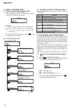
6. Set the laser power meter so that the laser beam from the optical

pick-up aims at the objective lens of laser power meter at right
angle. (Confirm it with the disc not inserted)

7. Confirm that the value of laser power meter is 0.860 mW 

±

19.2%.

8. Press the  

>

  key to select the item number 9112.

9. Confirm that the value of laser power meter is 0.763 mW 

±

18.2%.

10. Press the  

>

  key to select the item number 9113.

11. Confirm that the value of laser power meter is 6.87 mW 

±

12%.

12. Press the  

x

  key four times and back to the Display Check

mode.

3-5. Setting The  Adjustment Values
3-5-1. Hi-MD3 setting

Preparation:

1. Perform calculation every item based on the data given by the

Hi-MD3 adjustment disc by referring to the following table.
(Round off the value in decimal place)

2. Convert the calculated value into hexadecimal number.

Note:

The Hi-MD3 adjustment parameters vary depending on the disc,
and therefore use the parameters of the disc used when performing
the adjustment.

Item No.

Calculating formula (

*

3)

0211

Pr_nominal / 0.05

(*1)

Por / 0.05

0212

Kr 

×

 (

100)

0213

Pw_nominal / 0.05

(*2)

Ppw / 0.05

0214

Kw 

×

 (

100)

0215

Prmin / 0.05

0216

Pwmin / 0.05

5. Press the  

>

  key three times to select the item number 9111

and display as follows.

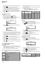
Display

9 0 0 0
D E S I G N

9 1 1 1
L r e f P w   * *

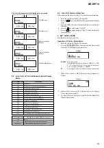
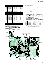
7. Select the item number 2244, and turn off the power supply of

battery terminal.

8. Press the  

>

  key to select the item number 2245.

9. Adjust with 

[VOL+]

/

[VOL--]

 keys so that the voltage of between

CL935 and CL433 (GND) becomes 1.80 V 

(−

 0.02 V).

10. Apply the voltage of 1.2 V to the battery terminal again.
11. Turn off the voltage of 5 V to the CL453 and CL460 (GND).
12. Press the  

x

  key three times and back to the Display Check

mode.

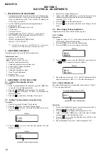
3-4. Laser Power Check

Procedure:

1. Enter the test mode (Display Check mode).
2. Press the 

[VOL+]

 key to enter the Manual mode.

3. Open the lid and press the  

.

  key continuously until the

optical pick-up moves to the most inward track.

4. Press the 

[VOL--]

 key once to display as follows.

Display

*1) If the “Pr_nominal” value is indicated, use the “Pr_nominal” value

and not used “Por” value.

*2) If the “Pw_nominal” value is indicated, use the “Pw_nominal” value

and not used “Ppw” value.

*3) Round off after the decimal point.

Table 3-5-1. Hi-MD3 adjustment parameter

Example of Calculation:

Item No.

Parameter

Result

Decimal

Hexadecimal

0211

Pr_nominal

2.48 mW

50

32h

0212

Kr

0.3 %/

°

C

30

1Eh

0213

Pw_nominal

7.35 mW

147

93h

0214

Kw

0.4 %/

°

C

40

28h

0215

Prmin

1.9 mW

38

26h

0216

Pwmin

5.8 mW

116

74h

Procedure:

1. Enter the test mode (Display Check mode).
2. Press the 

[VOL+]

 key to enter the Manual mode.

3. Press the  

>

  key once, press the 

[VOL+]

 key once, and press

the  

>

  key once again to display as follows.

Display

4. Press the 

[VOL+]

/

[VOL--]

 key and set the according value to

each destination referring to the following table.

5. Press the  

X

  key to write the adjusted value.

6. Press the  

>

  key to select the item number 0114.

7. Repeat adjustment from step 3.
8. Press the  

x

  key four times and back to the Display Check

mode.

Destination

Setting value

Item No. 0113 Item No. 0114

US and Canadian

20

80

Table 3-5-2. Destination Setting

4. Press the  

>

  key once to select the item number 0211.

5. Adjust with 

[VOL+]

/

[VOL--]

 keys so that the adjustment value

of LCD becomes calculated value.

6. Press the  

X

  key to write the adjusted value.

7. Press the  

>

  key to next item.

8. Repeat adjustment from step 4 until item number 0216.

3-5-2. Destination setting

Procedure:

1. Enter the test mode (Display Check mode).
2. Press the 

[VOL+]

 key to enter the Manual mode.

3. Press the  

>

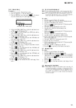
  key five time to select the item number 0113

and display as follows.

Display

0 2 1 0
D i s c P r

0 1 1 3
D i s t F L   * *

adjustment value (hexadecimal)

Ver. 1.1

Содержание Hi-MD WALKMAN MZ-DH710

Страница 1: ...her trademarks and registered trademarks are trademarks or registered trademarks of their respective holders and marks are omitted in this manual CD and music related data from Gracenote Inc copyright 2000 2004 Gracenote Gracenote CDDB Client Software copyright 2000 2004 Gracenote This product and service may practice one or more of the following U S Patents 5 987 525 6 061 680 6 154 773 6 161 132...

Страница 2: ...mensions Approx 83 6 29 5 77 0 mm w h d 33 8 13 16 31 8 in excluding projecting parts and controls Mass Approx Supplied accessories Earphones Dedicated USB cable CD ROM SonicStage MD Simple Burner Recordable disc Do not play a CD ROM on an audio CD player 107 g 3 8 oz the player only Design and specifications are subject to change without notice Revolutions 350 rpm to 3 000 rpm CLV Error correctio...

Страница 3: ... 8 3 6 Set Chassis Assy 9 3 7 Gear BSA Gear SB 9 3 8 OP Service Assy 10 3 9 DC Motor SSM18D C NP Spindle M701 DC Motor Sled M702 DC Motor Unit Over Write Head Up Down M703 10 3 10 Holder Assy 11 3 11 Position of Ferrite Core 11 4 TEST MODE 12 5 ELECTRICAL ADJUSTMENTS 16 6 DIAGRAMS 6 1 Block Diagram MD SERVO Section 21 6 2 Block Diagram POWER SUPPLY Section 22 6 3 Printed Wiring Board MAIN Section ...

Страница 4: ...er bridges occur such as on IC pins etc Usable with ordinary solder It is best to use only unleaded solder but unleaded solder may also be added to ordinary solder Providing the required system environment The following system environment is required in order to use the SonicStage Ver 3 0 MD Simple Burner Ver 2 0 software for the MD Walkman This software is not supported by the following environme...

Страница 5: ...witch in the direction of the arrow to disable the buttons on the player To prevent the buttons from being accidentally operated when you carry the player use this function L i earphones jack The display window of the player A Character information display Displays the disc and track names date error messages track numbers etc B Hi MD MD indication Hi MD lights up when the operation mode of the pl...

Страница 6: ... MD STANDARD PIN Page 8 3 7 GEAR BSA GEAR SB Page 9 3 11 POSITION OF FERRITE CORE Page 11 3 8 OP SERVICE ASSY Page 10 3 9 DC MOTOR SSM18D C NP SPINDLE M701 DC MOTOR SLED M702 DC MOTOR UNIT OVER WRITE HEAD UP DOWN M703 Page 10 3 10 HOLDER ASSY Page 11 3 6 SET CHASSIS ASSY Page 9 SET Note 1 The process described in can be performed in any order Note 2 Without completing the process described in the ...

Страница 7: ...crews M1 4 1 Remove two solders 3 flexible board CN471 2 flexible board CN701 6 flexible board CN501 7 MAIN board 5 3 2 CASE LOWER SECTION 2 Remove the case lower section in the direction of the arrow 1 two screws M1 4 1 two screws M1 4 ...

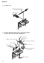
Страница 8: ...ection 6 boss 3 torsion spring pop up L 2 Open the case upper section 1 flexible board CN471 4 two step screws 5 3 5 MECHANISM DECK SECTION MT MZNH900 181 MD STANDARD PIN 2 mechanism deck section MT MZNH900 181 3 MD standard pin 1 two step screws MD ...

Страница 9: ...GEAR BSA GEAR SB 1 torsion coil spring R 2 extension spring R 5 two screws 3 compression coil spring limitter 4 open slider 6 battery case 7 set chassis assy 1 self tap screw 2 thrust retainer spring 3 washer 0 8 2 5 4 gear BSA 5 gear SB ...

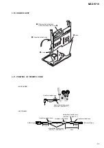
Страница 10: ... screw block assy is turned and it removes from OP service assy 2 OP service assy 3 two screws M1 4 4 DC motor sled M702 1 Remove four solders of flexible board 2 Remove two solders of flexible board 6 three self tap screws 7 DC motor SSM18D C NP spindle M701 5 motor base assy 9 DC motor unit over write head up down M703 8 self tap screw ...

Страница 11: ...3 11 POSITION OF FERRITE CORE USB A type USB mini B type EARPHONES USB CABLE A cable is rolled twice A cable is rolled twice A cable is rolled once A cable is rolled once clamp filter ferrite core Part No 1 400 878 11 clamp filter ferrite core Part No 1 400 877 11 clamp filter ferrite core Part No 1 400 877 11 1cm 4cm 4cm 4cm ...

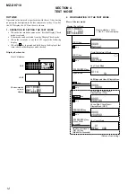
Страница 12: ...ION 4 TEST MODE Manual Mode Sound Skip Check Result Display Mode Play Display Check Mode Version display All lit All off Version display VOL key x key x key N ENT key Self Diagnosis Result Display Mode x key key Sound Skip Check Result Display Mode REC x key Key Check Mode SEARCH MENU key Overall Adjustment Mode VOL key x key Open the lid Key Count Mode SEARCH MENU key press a few seconds Not used...

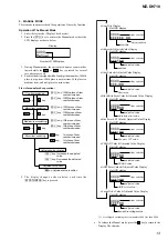
Страница 13: ... item number decrease Minor item switching VOL key Increases the adjusted value VOL key Decreases the adjusted value Adjusted value variation Adjusted value write key Adjusted value is written X 5 The display changes a shown below each time the SEARCH MENU key is pressed Address Adjusted Value Display Set LCD display Set LCD display Set LCD display item number item title adjusted value Jitter Valu...

Страница 14: ...y mode you can determine when the error occurred Clear the total recording time if the optical pick up was replaced 5 1 Operation of The Self Diagnosis Result Display Mode 1 Enter the test mode Display Check mode 2 Press the key to activate the Self Diagnosis Result Display mode where the LCD displays as shown below Display 4 OVERALL ADJUSTMENT MODE 4 1 Operation of The Overall Adjustment Mode 1 E...

Страница 15: ...cluster specified when error occurs 002 to 034 Total recording time when erroe occurs Flow of Self diagnosis Result Display mode operation The first error VOL key VOL key The last error VOL key VOL key One error before the last VOL key VOL key Two error before the last VOL key VOL key Total recording time VOL key VOL key 1 N N1 N2 R_ 5 3 Clear The Total Recording Time After replacing the optical p...

Страница 16: ...tering the test mode Note Enter the test mode with a key 2 Initialize the adjustment value 3 Setting the temperature correction value 4 Power supply voltage adjustment 5 Laser power check 6 Setting the adjustment values 7 Servo Overall adjustment 8 Resume clear 9 Releasing the test mode 3 ADJUSTMENT OF THE EACH ITEM 3 1 Initialize The Adjustment Value Procedure 1 In the test mode Display Check mod...

Страница 17: ...39 R525 R526 C661 C660 R650 R635 C553 C518 L503 D611 Q615 Q901 Q614 K A Q613 G D S L907 L906 L901 FB801 C634 R648 R406 R677 R664 L608 R649 C628 R845 C674 X801 D801 Q802 Q609 A K S D G Q801 D803 A K C622 C627 C616 C614 C613 L601 D602 K A D603 A K Q612 S D G SL901 L603 L701 L702 CN701 C423 C424 L605 C653 C612 C621 C356 C643 Q611 Q608 E C B Q607 D604 A K C658 C354 F351 D609 D613 D610 A K A K IC601 C6...

Страница 18: ...ocedure 1 Enter the test mode Display Check mode 2 Press the VOL key to enter the Manual mode 3 Open the lid and press the key continuously until the optical pick up moves to the most inward track 4 Press the VOL key once to display as follows Display 1 If the Pr_nominal value is indicated use the Pr_nominal value and not used Por value 2 If the Pw_nominal value is indicated use the Pw_nominal val...

Страница 19: ...ume clear 5 Press the x key four times and back to the Display Check mode 3 8 Releasing The Test Mode Note When the power supply is switched on in the state where all electrical adjustments have not finished it is displayed on LCD as Error EE and the usual operation can t be performed When a power supply is accidentally turn off in the middle of electrical adjustments it is again set as test mode ...

Страница 20: ...20 MZ DH710 MEMO ...
Страница 21: ... MON U CLV MON V CLV MON W SPRD SPDL_MON SLDW SLDV SRDR SLD_MON FRDR FFDR TRDR TFDR SPDV SPDW XRST_MTR_DRV RI1 FI1 RI2 FI2 WI2 VI2 UI2 VI1 WI1 CPWO2 CPVO2 CPUO2 SLD MON W SLD MON V SLD MON U STALL UI1 PWM1 FO2 FCS FCS TRK TRK COM2 WO1 CPVI2 WO2 CPUI2 CPWI2 CPUI1 CPVI1 CPWI1 COM1 FOCUS TRACKING COIL DRIVE SPINDLE SLED MOTOR DRIVE IC701 M701 SPINDLE 11 RF_IY 10 RF_IX 26 CLK 174 FS256_OUT PLSE_XDC CO...

Страница 22: ...Y PAUSE 124 SET_KEY_1 SET_KEY_1 125 SET_KEY_2 SET_KEY_2 213 SI1 SDI 214 SO1 SDO 215 SCK1 SCK 236 XCS_LCD CS SWITCH UNIT 192 XRST_LCD RST XWK RESET SWITCH Q471 DVDD DDC3 B 2 4V REGULATOR IC471 RESET SIGNAL GENERATOR IC902 1 2V REGULATOR IC604 VOLTAGE DETECT IC606 OR GATE IC605 WAKE UP SWITCH Q902 136 XRST 141 DACVREFH VB B 5 XWK1 GROUND LINE SWITCHING Q403 406 VBUS B SWITCH Q901 B SWITCH Q352 353 B...

Страница 23: ... to normal produc tion tolerances Waveforms are taken with a oscilloscope Voltage variations may be noted due to normal produc tion tolerances Circled numbers refer to waveforms Signal path E PLAYBACK j REC d USB input from PC G USB output to PC Note on Printed Wiring Board X parts extracted from the component side Y parts extracted from the conductor side f internal component Pattern from the sid...

Страница 24: ...4 C570 C402 C403 Q601 Q602 Q603 R668 C919 C453 C452 FB503 FB502 C906 C918 R680 C480 C481 Q616 Q617 D614 K A D605 A K D608 A K L606 R491 R490 R489 R486 R480 R476 R477 R424 R421 R423 R422 C716 R707 R706 C701 LF301 R351 R156 R160 R260 R256 C353 D151 A K 1 3 5 4 IC471 L9001 L351 C352 C160 C260 L607 Q403 Q406 Q451 C924 Q452 Q502 B C E E C B Q503 IC701 D458 K A D440 K A J352 CN451 USB CN451 FRONT VIEW D...

Страница 25: ...5 6 7 8 9 10 11 57 56 54 52 49 45 41 37 34 32 30 29 58 59 55 53 50 46 42 38 35 33 31 28 84 87 89 91 94 98 102106 109 111 3 2 85 86 88 90 93 97 101105 108 110 112 1 62 63 64 51 47 43 39 36 25 24 65 66 67 68 48 44 40 23 22 21 77 78 79 96 100104 12 11 10 9 80 81 92 95 99 103107 8 7 6 69 70 71 72 20 19 18 17 73 74 75 76 16 15 14 13 60 61 27 26 82 83 5 4 5451 48 45 43 42 40 37 34 31 5552 49 47 44 41 38...

Страница 26: ...SLD_PWM SLD_CON_U SLD_CON_V SLD_CON_W XRST_MTR_DRV SLD_CON_W SLD_CON_V SLD_CON_U SLD_PWM SLD_MON_U SLD_MON_V SLD_MON_W CLV_CON_U CLV_CON_V CLV_PWM CLV_MON_U CLV_MON_V CLV_MON_W CLV_CON_W CLV_CON_W CLV_CON_V CLV_CON_U CLV_PWM CLV_MON_U CLV_MON_V CLV_MON_W FF1 TF1 TR1 FR1 FF1 FR1 TF1 TR1 ZI1 ZI2 ZI1 ZI2 HD_DRV HD_DRV CLVW CLVV CLVU CLVN SLEDN SLEDU SLEDV SLEDW VI2 UI2 PWM2 CPUO2 CPVO2 CPWO2 STALL GN...

Страница 27: ...P4601 TXE 1M 1M 10k 10k 1M 4700p 0 047 MA2SD30 MA2SD30 MA22D17 33p 100V A1 A2 A3 A4 A5 C1 C2 E1 E2 E3 E4 E5 E6 E7 E8 E9 E10 E11 E13 F1 D1 F2 VB RMC_DTCK VBUS_VB_CTL XCS_REC_DRV VBUS_DET DDC3 REG_F EFM_CLK EFM RECP SUSPEND USB_HOLD 3 3V 4FS SDO0 SCK0 RST_CONT SLEEP VREC_SEL XRST REG5_REG REG5_VSTB REG5_OSC REG4_DVDD REG_DACVREFH VREC_SEL XCS_REC_DRV XCS_REC_DRV VBUS_DET VBUS_DET REG_F REG_F EFM_CLK...

Страница 28: ...1 0 1 0 2SC4627J C TX SO SN761059AZQLR 0 1 10 B1 B2 B3 C1 C2 I1 I2 REG03 PEAK PLSE_XDC XLDON BOTM OFTRK MDVCC_CTL RFI VIN ADIP VC S_MON APCREF_DA SSB_DATA SSB_CLK XRST_RF VREF ABCD FE TE A_FS256 S1 S0 PEAK PEAK PLSE_XDC PLSE_XDC XLDON XLDON BOTM BOTM OFTRK OFTRK MDVCC_CTL MDVCC_CTL RFI RFI VIN VIN VC ADIP ADIP VC S_MON S_MON APCREF_DA APCREF_DA TE FE ABCD VREF XRST_RF SSB_DATA SSB_CLK SSB_DATA SSB...

Страница 29: ...TQ035P02TR SI1410EDH T1 0 1 0 1 1000p 220 5V 220 5V 1M 470k 100k 0 1 0 1 XP4601 TXE 220k MA8056 L TX 10k 0 047 220 5V 220 5V 220k 1M MA22D2800SL0 7P 0 1 0 1 0 1 2200p MA22D2800SL0 2 2M 100k 220 470k 0 1 XP4601 TXE MAZS027008SO GND 2200p 0 GND 015AZ4 7 TPL3 0 D1 G1 G2 G3 H1 UDP UDM GND_SW VBUS_MON MINUS_MON UDM UDP UDP UDM S VBUS DATA DATA IO GND SW_A SW_B S 1 2 Q403 406 GROUND LINE SWITCHING Q451 ...

Страница 30: ...H L9001 10µH MA2Z748001S0 10 6 3V 100 6 3V 47 6 3V 1000p 10k 100p 1000p 220k 470k 470k 470k 2 2k 470k 0 0 2 2 0 01 0 0 4 7 220k 22k 100k 1000p 2 2 2 2 100k 47k 2 2 22k 47k 100p MA22D2800LS0 47k 0 1 XP4601 TXE TS8K1TB 47k 22 6 3V 22 6 3V 2 2 22 6 3V XC61CC1702NR 0 1 22k 22k 1k 47k 100k 100k 100k E1 E2 E3 E4 E5 E6 E7 E8 E9 E10 E11 E13 G1 G2 G3 I1 I2 J1 J2 J3 J4 J5 SDO0 SCK0 4FS XCS_PWR_IC XRST2 WK_D...

Страница 31: ...7k 4 7k 2 2 10 4V 1 4 7 4V 22k 10k 100k 2 2M 1M 0 220k 10 6 3V 0 NNCD6 8H T1 02DZ2 4 Z TPH3 02DZ2 4 Z TPH3 0 25A 125V 2SC4738F Y GR TPL3 0 01 0 1 XP4314 TX 0 0 F1 H1 J1 J2 J3 J4 J5 F2 S_GND XHP_STBY BEEP MUTE AOUTR AOUTL RMC_KEY XCS_PWR_IC WK_DET REC_KEY HALF_LOCK XRST2 GND BEEP MUTE XHP_STBY AOUTR AOUTL BEEP MUTE XHP_STBY AOUTR AOUTL RMC_KEY RMC_KEY XCS_PWR_IC WK_DET REC_KEY HALF_LOCK XRST2 2 2 1...

Страница 32: ...TB REG5_OSC REG4_DVDD XCS_PWR_IC WK_DET REC_KEY HALF_LOCK XRST2 S_GND GND REG_DACVREFM REG5_REG REG5_VSTB SDI0 XCS_NV SDO0 SCK0 WK_DET REC_KEY HALF_LOCK XRST2 RMC_KEY XCS_PWR_IC XCS_LCD SDI1 SDO1 SCK1 LCD_RST JOG_B JOG_A SET_KEY_2 SET_KEY_1 REC_KEY WK_DET XHOLD_SW PAUSE XRST2 RMC_DTCK 4FS SDO0 SCK0 RST_CONT SLEEP VREC_SEL XRST REG_F REG5_REG 3 3V REG5_VSTB REG5_OSC REG4_DVDD HIMD_PROTECT PROTECT H...

Страница 33: ...TL A_FS256 VIN REG4_DVDD 3 3V REG_F REG5_VSTB REG5_OSC REG5_REG REG5_REG JOG_A JOG_B HIMD_PROTECT ZI2 ZI1 REG_DACVREFM XLDON VBUS_VB_CTL GND_SW VBUS_MON MINUS_MON XRST_MTR_DRV RECP SCK1 SDO1 RMC_DTCK S0 S1 S1 S0 VOUT VIN VSS NC DVDD1_0 DVSS1_0 DVDD1_1 DVSS1_1 DVDD1_2 DVSS1_2 DVDD1_3 DVSS1_3 DVDD1_4 DVSS1_4 DVDD1_5 DVSS1_5 DVDD1_6 DVSS1_6 DVDD1_7 DVSS1_7 DVDD1_8 DVSS1_8 DVDD1_9 DVSS1_9 DVDD1_10 DVS...

Страница 34: ...T 99 SUS IN 100 PGND2 101 TSBV IN 102 TSBV OUT 103 V33R 104 PGND1 105 VSTB IN 106 VSTB OUT 107 BATSEL 108 V33RO 109 RF1 110 INM1 111 DTC1 112 VREC HOLD LOGIC BUFFER CHARGE PUMP PVBUS VG VREC POWER SWITCH DRIVER CIRCUIT 2 0V RESET RESET LOGIC VREC STEP UP DOWN CONVERTER DRIVER PWM V3 STEP UP DOWN CONVERTER DRIVER PWM VC V3FB VREF BUFFER DAC VPDRV VBUS VBUS VG3 VIF H BRIDGE DRIVER CONTROL SYSTEM BUS...

Страница 35: ...ND1 14 RO1 13 RO1 16 FO1 32 FO2 19 FI1 20 RI1 29 RI2 30 FI2 21 COM1 22 CPUI1 23 CPVI1 VG PRE DRIVE VG VG VG PRE DRIVE VG PRE DRIVE 24 CPWI1 25 CPWI2 26 CPVI2 27 CPUI2 28 COM2 33 FO2 34 PGND2 37 VMR2 38 VMU2 39 UO2 40 UO2 42 VO2 43 VO2 46 WO2 45 ST2 44 VMVW2 47 PGNDW2 48 WI2 41 PGNDUV2 35 RO2 36 RO2 IC892 HN58X2564FPIEZ 1 8 7 6 5 2 3 4 Y DECODER X DECODER ADDRESS GENERATOR HIGH VOLTAGE GENERATOR ME...

Страница 36: ...VGSEL1 28 VGSEL2 30 INM2 31 RF2 32 DTC2 RST2 REF2 VG SELECT VG DUTY CLK 36 PGND2 35 PGND2 L2 37 L2 38 VO2 39 VCO2 40 VCIN 41 VC2 42 DW 2T 43 DW 2B 44 MUTEON 45 REGC3 46 REGO3 47 REGI3 48 SERIAL PASS REGULATOR 2 SERIAL PASS REGULATOR 1 RST1 RST2 SEQSEL MUTE ON MUTING BUFFER VC2 RST2 POWER SWITCH 1 RST2 STEP UP DOWN DRIVER PWM START UP RESET 2 VC2 REF2 VREF VB REF1 VC VREF 27 VB STEP UP DC DC CONVER...

Страница 37: ... DVDD1_10 Power supply terminal 24 DVSS1_10 Ground terminal 25 DVDD1_11 Power supply terminal 26 DVSS1_11 Ground terminal 27 AVDD1A Power supply terminal for PLL 28 AVSS1A Ground terminal for PLL 29 AVDD1B Power supply terminal 30 AVSS1B Ground terminal 31 AVDD1C Power supply terminal 32 AVDD2 Power supply terminal for A D converter 33 DVDD25SVADC Power supply terminal for A D converter 34 AVSS2 G...

Страница 38: ... supply terminal for AUX 78 FVSS0 Ground terminal for AUX 79 SRAMVDD0 Power supply terminal for AUX 80 SRAMVSS0 Ground terminal for AUX 81 SRAMVDD1 Power supply terminal for AUX 82 SRAMVSS1 Ground terminal for AUX 83 EBIFVDD0 Power supply terminal for interface circuit 84 EBIFVSS0 Ground terminal for interface circuit 85 EBIFVDD1 Power supply terminal for interface circuit 86 EBIFVSS1 Ground termi...

Страница 39: ...r for class D amplifier Not used 121 VB_MON I Unregulated power supply voltage monitoring terminal 122 CHG_MON I Charge or discharge current monitoring terminal Not used 123 VREF_MON O Reference voltage output terminal 124 SET_KEY_1 I Front panel key input terminal 125 SET_KEY_2 I Front panel key input terminal 126 DCIN_DET I DC input voltage for battery charge monitoring terminal Not used 127 HID...

Страница 40: ...e motor driver 166 SPCW I Spindle motor drive comparison signal input W from the motor driver 167 SLDV O Sled motor drive control signal output V to the motor driver 168 SLDW O Sled motor drive control signal output W to the motor driver 169 SLCU I Sled motor drive comparison signal input U from the motor driver 170 SLCV I Sled motor drive comparison signal input V from the motor driver 171 SLCW I...

Страница 41: ...odule 216 SLD_MON I Sled servo monitoring terminal 217 AOUT_SEL O Headphone line output switching terminal Not used 218 YUZU_SLEEP O Chip enable output to the power control IC 219 FFCLR O Input latch output for the start switching to the power control Not used 220 CHGI_CTL1 O Charge current limiter control signal output at the time of DC adaptor use L charge Not used 221 CHGI_CTL2 O Charge current...

Страница 42: ...arging Not used 256 DRAM_HOLD _DET I Detection terminal for D RAM power supply information keeping Not used 257 DRAM_VDD _CLR O D RAM power latch clear signal output for quick mode sleep Not used 258 AD2ENDF I Monitoring terminal for flag of servo signal A D measuring finish 259 TEST Not used 260 SRAM_MODE I Not used 261 HSALF I Not used 262 to 271 TIGER_MON0 to TIGER_MON9 O Trigger monitoring ter...

Страница 43: ...put terminal 13 5 MHz or 27 MHz Not used 306 FS256 O Master clock signal 256Fs 11 2896 MHz output to external A D D A converter Not used 307 ADDT I Data input from external A D converter Not used 308 LRCK O L R sampling clock signal 44 1kHz output to external A D D A converter Not used 309 XBCK O Bit clock 2 8224 MHz output to the external A D D A converter Not used 310 OSCI I Main system clock in...

Страница 44: ...not supplied Accessories are given in the last of the electrical parts list NOTE XX and X mean standardized parts so they may have some difference from the original one Color Indication of Appearance Parts Example KNOB BALANCE WHITE RED Parts Color Cabinet s Color 6 3 266 359 01 SPRING POP UP L TORSION 7 3 241 529 01 SCREW STEP case upper section chassis section not supplied 6 1 1 1 7 2 3 5 Les co...

Страница 45: ...CKER OPEN 54 2 541 973 01 KNOB ROTARY 55 3 266 192 01 ESCUTCHEON 5 DIRECTION VOL VOL 56 3 266 191 01 KNOB 5 DIRECTION B ENT 57 2 541 972 01 BUTTON CONTROL DOWNLOAD X SEARCH MENU CANCEL 58 2 541 969 01 HOLDER LCD 59 2 022 247 01 RUBBER CONDUCTIVE 60 A 1104 958 A SWITCH BOARD COMPLETE 61 3 254 014 01 SCREW LCD101 1 805 632 11 LCD 51 52 53 54 55 56 57 58 59 60 61 61 LCD101 SWITCH board ...

Страница 46: ...96 01 SCREW MD STEP 110 X 2059 302 1 MAIN BOARD COMPLETE for SERVICE Canadian 110 X 2059 303 1 MAIN BOARD COMPLETE for SERVICE US 111 3 238 876 04 SCREW M1 4 TOOTHED LOCK 112 3 266 204 01 TERMINAL BATTERY 113 3 266 203 02 TERMINAL BATTERY 114 2 109 025 02 SHEET PWB LINE 115 2 109 021 01 SHEET PWB HP 116 2 109 024 01 SHEET PWB DC 118 2 541 975 01 SPRING USB LEAF 120 2 176 386 01 SHEET SET CHASSIS L...

Страница 47: ...972 24 CHASSIS REC 158 X 3384 651 2 BASE ASSY MOTOR 159 X 3384 650 3 HOLDER ASSY 160 3 263 453 01 PLATE RATCHET 161 X 2023 272 1 SERVICE ASSY LEAD SCREW 162 3 244 879 01 SPRING RACK 0163 X 2055 997 1 OP SERVICE ASSY ABX U including HR601 OVER WRITE HEAD M701 8 835 782 12 MOTOR DC SSM18D C NP SPINDLE M702 1 787 143 11 MOTOR DC SLED M703 1 477 519 21 MOTOR UNIT DC OVER WRITE HEAD UP DOWN M701 M703 M...

Страница 48: ...5 210 11 TANTALUM CHIP 4 7uF 20 10V C519 1 125 777 11 CERAMIC CHIP 0 1uF 10 10V C520 1 125 777 11 CERAMIC CHIP 0 1uF 10 10V C521 1 164 850 11 CERAMIC CHIP 10PF 0 5PF 50V C522 1 164 850 11 CERAMIC CHIP 10PF 0 5PF 50V C523 1 125 777 11 CERAMIC CHIP 0 1uF 10 10V C524 1 162 970 11 CERAMIC CHIP 0 01uF 10 25V C525 1 164 941 11 CERAMIC CHIP 0 0047uF 10 16V C526 1 164 874 11 CERAMIC CHIP 100PF 5 50V C527 ...

Страница 49: ...23 11 CERAMIC CHIP 0 047uF 10 10V C705 1 164 943 11 CERAMIC CHIP 0 01uF 10 16V C706 1 107 819 11 CERAMIC CHIP 0 022uF 10 16V C707 1 164 943 11 CERAMIC CHIP 0 01uF 10 16V C708 1 107 819 11 CERAMIC CHIP 0 022uF 10 16V C709 1 164 943 11 CERAMIC CHIP 0 01uF 10 16V C710 1 107 819 11 CERAMIC CHIP 0 022uF 10 16V C712 1 125 777 11 CERAMIC CHIP 0 1uF 10 10V C713 1 125 777 11 CERAMIC CHIP 0 1uF 10 10V C714 ...

Страница 50: ...00LS0 D608 6 500 910 01 DIODE MA2SD3000LS0 D609 8 719 072 27 DIODE MA2Z748001S0 D610 8 719 072 27 DIODE MA2Z748001S0 D611 8 719 072 27 DIODE MA2Z748001S0 D613 6 500 813 01 DIODE MA2SD32008S0 D614 6 500 813 01 DIODE MA2SD32008S0 D615 6 500 909 01 DIODE MA22D1700LS0 D616 6 500 909 01 DIODE MA22D1700LS0 D801 8 719 072 27 DIODE MA2Z748001S0 D803 6 500 813 01 DIODE MA2SD32008S0 D902 8 719 072 27 DIODE ...

Страница 51: ...6W R153 1 218 965 11 RES CHIP 10K 5 1 16W R154 1 218 965 11 RES CHIP 10K 5 1 16W R155 1 218 929 11 RES CHIP 10 5 1 16W R156 1 218 961 11 RES CHIP 4 7K 5 1 16W R157 1 208 683 11 METAL CHIP 1K 0 5 1 16W R158 1 208 691 11 METAL CHIP 2 2K 0 5 1 16W R160 1 218 990 11 SHORT CHIP 0 R251 1 218 965 11 RES CHIP 10K 5 1 16W R252 1 218 957 11 RES CHIP 2 2K 5 1 16W R253 1 218 965 11 RES CHIP 10K 5 1 16W R254 1...

Страница 52: ...TAL CHIP 2 2 5 1 10W R665 1 218 990 11 SHORT CHIP 0 R668 1 216 864 11 SHORT CHIP 0 R670 1 218 990 11 SHORT CHIP 0 R671 1 218 990 11 SHORT CHIP 0 R673 1 218 990 11 SHORT CHIP 0 R675 1 220 804 11 RES CHIP 2 2M 5 1 16W R677 1 216 864 11 SHORT CHIP 0 R679 1 218 945 11 RES CHIP 220 5 1 16W R680 1 216 864 11 SHORT CHIP 0 R681 1 218 989 11 RES CHIP 1M 5 1 16W R682 1 218 989 11 RES CHIP 1M 5 1 16W R683 1 ...

Страница 53: ...3 11 METAL CHIP 220K 0 5 1 16W R934 1 208 715 11 METAL CHIP 22K 0 5 1 16W R935 1 208 935 11 METAL CHIP 100K 0 5 1 16W R936 1 208 927 11 METAL CHIP 47K 0 5 1 16W R937 1 208 715 11 METAL CHIP 22K 0 5 1 16W R938 1 208 927 11 METAL CHIP 47K 0 5 1 16W R951 1 218 990 11 SHORT CHIP 0 R952 1 218 990 11 SHORT CHIP 0 R953 1 220 803 81 RES CHIP 4 7 5 1 16W R954 1 218 985 11 RES CHIP 470K 5 1 16W R955 1 218 9...

Страница 54: ...allows you to jump to the revised page Also clicking the version at the top of the revised page allows you to jump to the next revised page Ver Date Description of Revision 1 0 2005 04 New 1 1 2010 10 Correction of Destination setting value SMR 10048 ...

Отзывы: