15
15
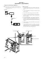
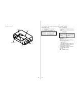
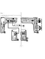
• FOCUS GAIN ADJUSTMENT
(COARSE ADJUSTMENT)
This adjustment is to be performed when replacing the following
parts.
• Optical Pick-up Block
• RV14
– RF BOARD (Conductor Side) –
Procedure:
1. Set RV14 (RF board) to the standard position.
2. Check that there is not an abnormal amount of operation noise
(white noise) from the 2-axis devise. If there is, turn RV14
slightly clockwise.
– RF BOARD (Conductor Side) –
• When gain is lowered...
The set does not play because of no focus operation.
• When gain is highered...
Operation noise is heard due to a scratch or a dust, then opera-
tion will be unstable.
RV14
IC11
IC51
CNJ12
MIN side
(low gain)
MAX side
(high gain)
RV14 standard position
SECTION 6
ELECTRICAL ADJUSTMENTS
Note:
1.
Perform adjustments as given.
2.
Power supply voltage: DC14.4 V (more than 3A).
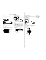
• FOCUS BIAS CHECK
– RF BOARD (Conductor Side) –
Procedure:
1. Connect the oscilloscope to TP (RF) and TP (VC) on the RF
board.
2. Put the set into play mode by loading the disc.
3. Confirm that oscilloscope waveform is clear and check RF sig-
nal level is correct or not.
Note:
Clear RF signal waveform means that the shape “
◊
” can be clearly distin-
guished at the center of the waveform.
• TRACKING OFFSET CHECK
– RF BOARD (Conductor Side) –
Procedure:
1. Connect the oscilloscope to BP11 (TE) and TP (VC) on the
RF board.
2. Put the set into play mode by loading the disc.
3. Press the
.
AMS
>
button, and check the traverse wave-
form*.
4. Confirm that the oscilloscope waveform is symmetrical on the
top and bottom in relation to 0 V dc, and check this level.
* Traverse waveform: This is the tracking error wave form appears
when crossing the track.
TP
(VC)
IC11
IC51
CNJ12
TP (RF)
oscilloscope
+
–
RF signal waveform
VOLT/DIV: 200 mV
TIME/DIV: 500 ns
level: 1.4
±
0.3 Vp-p
TP
(VC)
IC11
IC51
CNJ12
BP11
(TE)
oscilloscope
+
–
A
B
0 V
A=B
traverse waveform
(100 track jump waveform)
VOLT/DIV : 500 mV
TIME/DIV : 2 ms
Center : 0 V
Traverse waveform
Содержание CDX-838 - Compact Disc Changer System
Страница 3: ...3 SECTION 2 GENERAL This section is extracted from instruction manual ...
Страница 4: ...4 ...
Страница 5: ...5 ...
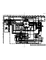
Страница 29: ...29 29 CDX 838 7 13 SCHEMATIC DIAGRAM DIGITAL OUT JACK Boards Page 25 ...

